SLAU863 October 2021 ADC12DJ4000RF , ADC12DJ5200RF , TRF1208
- Trademarks
- 1Features
- 2Equipment
-
3Setup Procedure
- 3.1 Install the High Speed Data Converter (HSDC) Pro Software
- 3.2 Install the Configuration GUI Software
- 3.3 Connect the EVM and TSW14J57EVM
- 3.4 Connect the Power Supplies to the Boards (Power Off)
- 3.5 Connect the Signal Generators to the EVM (Signal Generator's RF Outputs Disabled Until Directed)
- 3.6 Turn On the TSW14J57EVM Power and Connect to the PC
- 3.7 Turn On the ADCxxDJxx00RF-TRF1208-EVM Power Supplies and Connect to the PC
- 3.8 Turn On the Signal Generator RF Outputs
- 3.9 Open the ADC12DJ5200RFEVM GUI and Program the ADC and Clocks
- 3.10 Calibrate the ADC Device on the EVM
- 3.11 Open the HSDC Software and Load the FPGA Image to the TSW14J57EVM
- 3.12 Capture Data Using the HSDC Pro Software
- 4Device Configuration
- 5Troubleshooting the ADCxxDJxx00RF-TRF1208-EVM
- 6HSDC Pro Settings for Optional ADC Device Configuration
- 7Signal Routing
- 8References
- A Analog Inputs
- B Jumpers and LEDs
6.2.1 External Clocking Option (Default)
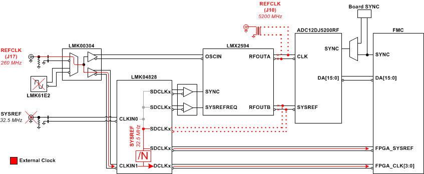
By default, the EVM is configured to use the external clock option. The user provide and external clock signal for both the ADC sampling clock (DEVCLK at J10) and also the reference clock (REF CLK at J17) which feed into the LMK04828 and is used in clock distribution mode and provides the FPGA reference clock, FPGA SYSREF signal and ADC SYSREF signal. If coherent sampling is desired the external clocking has to be used. Figure 6-1 shows the block diagram of external clocking option:
The EVM can be configured to use external clocks with the following steps (see Figure 6-4):
- Modify the hardware:
- Remove R171 and R174, populate C2 and C3.
- Remove C52 and C306, populate C60 and C61
- Install Jumper J13
 Figure 6-1 ADCxxDJxx00RF-TRF1208-EVM
Clocking System Block Diagram