SLCA005A May 2020 – July 2022 LM2903B-Q1
1.4 Pin Failure Mode Analysis (Pin FMA)
This section provides a Failure Mode Analysis (FMA) for the pins of the LM2903B-Q1. The failure modes covered in this document include the typical pin-by-pin failure scenarios:
- Pin short-circuited to Ground (see Table 1-6)
- Pin open-circuited (see Table 1-7)
- Pin short-circuited to supply (see Table 1-8)
- Pin short-circuited to an adjacent pin (see Table 1-9)
Table 1-6 through Table 1-9 also indicate how these pin conditions can affect the device as per the failure effects classification in Table 1-5.
Table 1-5 TI Classification of Failure Effects
| Class | Failure Effects |
|---|---|
| A | Potential device damage that affects functionality |
| B | No device damage, but loss of functionality |
| C | No device damage, but performance degradation |
| D | No device damage, no impact to functionality or performance |
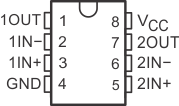
Figure 1-2 shows the pin diagram. For a detailed description of the device pins please refer to the 'Pin Configuration and Functions' section in the data sheet.
 Figure 1-2 Pin Diagram
Table 1-6 Pin FMA for Device Pins Short-Circuited to Ground
| Pin No. | Pin Name | Damage | Functionality | Description of Potential Failure Effect(s) | Failure Effect Class |
|---|---|---|---|---|---|
| 1 | OUT1 | No | Yes | No change if GND pin is GND node | B |
| 2 | 1IN- | No | Yes | Output goes high, if other input is positive | C |
| 3 | 1IN+ | No | Yes | Output goes low, if other input is positive | C |
| 4 | GND | No | Yes | No change if same node as GND | D |
| 5 | 2IN+ | No | Yes | Output goes low, if other input is positive | C |
| 6 | 2IN- | No | Yes | Output goes high, if other input is positive | C |
| 7 | OUT2 | No | Yes | No change if GND pin is GND node | B |
| 8 | VCC | No | No | Main supply shorted out (no power to device) | B |
Table 1-7 Pin FMA for Device Pins Open-Circuited
| Pin No. | Pin Name | Damage | Functionality | Description of Potential Failure Effect(s) | Failure Effect Class |
|---|---|---|---|---|---|
| 1 | OUT1 | No | Yes | Output can't drive application load | B |
| 2 | 1IN- | No | Yes | Output may be low or high | C |
| 3 | 1IN+ | No | Yes | Output may be low or high | C |
| 4 | GND | Possible | Affected | Lowest voltage pin will drive GND pin internally (via diode) | B |
| 5 | 2IN+ | No | Yes | Output may be low or high | C |
| 6 | 2IN- | No | Yes | Output may be low or high | C |
| 7 | OUT2 | No | Yes | Output can't drive application load | B |
| 8 | VCC | No | No | Main supply open (no power to device) | B |
Table 1-8 Pin FMA for Device Pins Short-Circuited to VCC
| Pin No. | Pin Name | Damage | Functionality | Description of Potential Failure Effect(s) | Failure Effect Class |
|---|---|---|---|---|---|
| 1 | OUT1 | Possible | Yes | Thermal stress due to high power dissipation | B |
| 2 | 1IN- | No | Yes | Output goes low, if other input is less positive | C |
| 3 | 1IN+ | No | Yes | Output goes high, if other input is less positive | C |
| 4 | GND | No | No | Main supply shorted out (no power to device) | B |
| 5 | 2IN+ | No | Yes | Output goes high, if other input is less positive | C |
| 6 | 2IN- | No | Yes | Output goes low, if other input is less positive | C |
| 7 | OUT2 | Possible | Yes | Thermal stress due to high power dissipation | B |
| 8 | VCC | No | Yes | No change if same node as VCC | D |
Table 1-9 Pin FMA for Device Pins Short-Circuited to Adjacent Pin
| Pin No. | Pin Name | Damage | Functionality | Description of Potential Failure Effect(s) | Failure Effect Class |
|---|---|---|---|---|---|
| 1 to 2 | OUT1 to IN1- | No | Yes | Output may be low or high | C |
| 2 to 3 | 1IN- to 1IN+ | Possible | Yes | Output may be low or high | C |
| 3 to 4 | 1IN+ to GND | No | Yes | Output goes low, if other input is positive | C |
| 4 to 5 | GND to 2IN+ | No | Yes | Output goes low, if other input is positive | C |
| 5 to 6 | 2IN+ to 2IN- | No | Yes | Output may be low or high | C |
| 6 to 7 | 2IN- to OUT2 | No | Yes | Output may be low or high | C |
| 7 to 8 | OUT2 to VCC | Possible | Yes | Thermal stress due to high power dissipation | B |
| 8 to 1 | VCC to OUT1 | Possible | No | Thermal stress due to high power dissipation | B |