SLDA021B March   2014  – February 2020 AM3892 , AM3894


  1.   1
    1.     2
    2.     3
      1.      4
        1.       5
      2.      6
    3.     7
      1.      8
        1.       9
      2.      10
        1.       11
        2.       12
          1.        13
      3.      14
      4.      15
    4.     16
      1.      17
      2.      18
      3.      19
      4.      20
    5.     21
      1.      22
        1.       23
      2.      24
      3.      25
      4.      26
      5.      27
      6.      28
      7.      29
      8.      30
    6.     31
      1.      32
      2.      33
      3.      34
      4.      35
      5.      36
      6.      37
    7.     38
      1.      39
      2.      40
      3.      41
      4.      42
    8.     43
      1.      44
      2.      45
      3.      46
      4.      47
    9.     48
      1.      49
      2.      50
      3.      51
      4.      52
      5.      53
      6.      54
      7.      55
        1.       56
        2.       57
      8.      58
      9.      59
      10.      60
    10.     61
    11.     62
      1.      63
      2.      64
    12.     65
  2.   66

Land Diameters and Solder Mask Opening Diameters

The primary board design considerations include metal-pad sizes and associated solder-mask openings. PCB pads/land patterns, which are used for surface mount assembly:

  • Non-solder mask defined (NSMD) — The metal pad on the PCB (to which a package BGA solder ball is attached) is smaller than the solder mask opening.

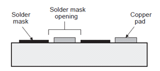
Figure 1 and Figure 2 illustrate the metal-pad and associated solder-mask openings

1Bitmap in nsmd_smd_slda021.pngFigure 1. NSMD Pads – Top View
1Bitmap in nsmd_smd_cross_slda021.pngFigure 2. NSMD – Cross-Sectional View