SLDU007C March 2012 – November 2015 PGA450-Q1
-
PGA450Q1EVM User’s Guide
- Trademarks
- 1 Read This First
- 2 EVM Overview
- 3 Power-Supply Requirements and Connections
- 4 Jumper Settings
- 5 Socket for Programming OTP
- 6 Transformer and Transducer
- 7 PGA450-Q1 Communication Interfaces
- 8 Controlling the PGA450-Q1 Memory Spaces With the GUI
- 9 LIN Master
- 10 Keil uVision Settings for Programming Firmware to the PGA450-Q1 DEVRAM or OTP Memory
- 11 Use Case
- 12 PGA450Q1EVM Schematics and Layout Drawings
- Revision History
11.1 Evaluation Through SPI Communication
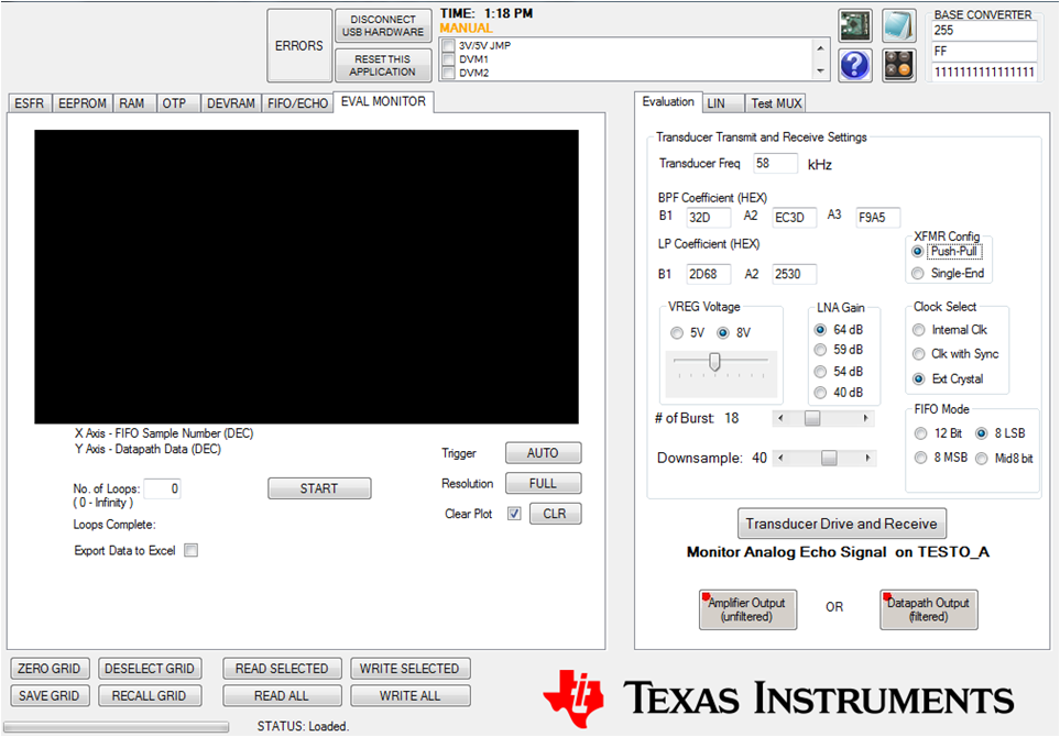
In order to provide a quick evaluation of the IC performance using the TI EVM and GUI without having to develop sophisticated 8051 µP software, the GUI provides an intuitive interface tab, Evaluation Tab, that collects all necessary information regarding the transducer drive and receive. For transducer drive, it includes: transducer frequency; transducer drive voltage, VREG; transformer configuration; and number of drive pulses. For transducer signal receive, it includes signal-processing parameters: LNA gain setting; BPF and LPF coefficient; clock selection; FIFO mode; and FIFO downsample size.
- Make sure all jumpers are connected according to the default settings, see Section 4.2.
- Connect the hardware and power supply, see Section 3. Make sure USB cable is connected to the computer and the interface board. It is recommended to monitor power supply current. Normal idle current is around 6 mA. Active current is around 15 mA.
- Launch GUI software on computer.
- Click the "OFF (Micro Reset)" button to put the Micro in reset, then click READ ALL to read the default register values. Some default values are loaded in the table grid. If all are 0 or FF values, this means that there is an error with communication to the device. Check the hardware setup or restart the GUI software.
Fill out the "Evaluation" tab with the values shown in Figure 15.
Use the "Eval Monitor" tab to send bursts and view the resulting echo data.
 Figure 15. Evaluation Tab Setting
 After all information is entered, make sure the device is in the micro reset state, then hit the Transducer Drive and Receive button to start the burst and receive.