SLDU007C March 2012 – November 2015 PGA450-Q1
-
PGA450Q1EVM User’s Guide
- Trademarks
- 1 Read This First
- 2 EVM Overview
- 3 Power-Supply Requirements and Connections
- 4 Jumper Settings
- 5 Socket for Programming OTP
- 6 Transformer and Transducer
- 7 PGA450-Q1 Communication Interfaces
- 8 Controlling the PGA450-Q1 Memory Spaces With the GUI
- 9 LIN Master
- 10 Keil uVision Settings for Programming Firmware to the PGA450-Q1 DEVRAM or OTP Memory
- 11 Use Case
- 12 PGA450Q1EVM Schematics and Layout Drawings
- Revision History
11.2 Monitoring the Signal Path
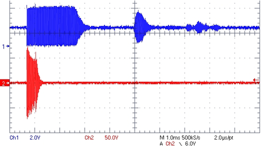
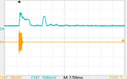
The PGA450-Q1 device has two useful test modes that allow users to quickly observe the echo signal as an amplified analog signal or from a DAC output which converts a digitally filtered echo signal. In the Evaluation tab, quick-access buttons Amplifier Output (unfiltered) and Datapath Output (filtered) are available. The signal is viewable on the DACO pin. Only one mode can be selected at a time. See Figure 16 and Figure 17 for the captured waveforms.
 Figure 16. Echo Analog Waveform Output (Channel1), Drive voltage (Channel 2)
  Figure 17. DAC Output of Filtered Signal (Channel 2) and Drive Voltage (Channel 1)