SLDU007C March   2012  – November 2015 PGA450-Q1


  1.   PGA450Q1EVM User’s Guide
    1.     Trademarks
    2. Read This First
    3. EVM Overview
    4. Power-Supply Requirements and Connections
      1. 3.1 Power Supply
      2. 3.2 Controlling and Powering the PGA450Q1EVM via the USB Interface Board
      3. 3.3 Connecting the Transducer
    5. Jumper Settings
      1. 4.1 Jumpers
      2. 4.2 Default Jumper Settings
      3. 4.3 0-Ω Resistors
    6. Socket for Programming OTP
    7. Transformer and Transducer
    8. PGA450-Q1 Communication Interfaces
      1. 7.1 SPI
      2. 7.2 LIN
      3. 7.3 UART
    9. Controlling the PGA450-Q1 Memory Spaces With the GUI
      1. 8.1 Using the Register Grids to Manipulate the Register Spaces
        1. 8.1.1 ZERO GRID
        2. 8.1.2 DESELECT GRID
        3. 8.1.3 SAVE GRID
        4. 8.1.4 RECALL GRID
        5. 8.1.5 READ SELECTED
        6. 8.1.6 WRITE SELECTED
        7. 8.1.7 READ ALL
        8. 8.1.8 WRITE ALL
      2. 8.2 ESFR Registers
      3. 8.3 EEPROM Registers
        1. 8.3.1 Program EEPROM
        2. 8.3.2 Reload EEPROM
      4. 8.4 RAM
      5. 8.5 OTP
        1. 8.5.1 Load .HEX File Into GUI
        2. 8.5.2 Program OTP Memory from .HEX File
        3. 8.5.3 Verify OTP Programming
        4. 8.5.4 Check OTP Status
      6. 8.6 DEVRAM
      7. 8.7 FIFO/ECHO
        1. 8.7.1 FIFO
        2. 8.7.2 EVAL Monitor
          1. 8.7.2.1 No. of Loops
          2. 8.7.2.2 Trigger
          3. 8.7.2.3 Resolution
          4. 8.7.2.4 Clear Plot
          5. 8.7.2.5 Export Data to Excel
          6. 8.7.2.6 Start/Stop
    10. LIN Master
    11. 10 Keil uVision Settings for Programming Firmware to the PGA450-Q1 DEVRAM or OTP Memory
      1. 10.1 Objective
      2. 10.2 Setup
    12. 11 Use Case
      1. 11.1 Evaluation Through SPI Communication
      2. 11.2 Monitoring the Signal Path
    13. 12 PGA450Q1EVM Schematics and Layout Drawings
  2.   Revision History

PGA450Q1EVM Schematics and Layout Drawings

schematic_LIN_sdu007.gifFigure 18. Schematic, LIN

spacer

spacer
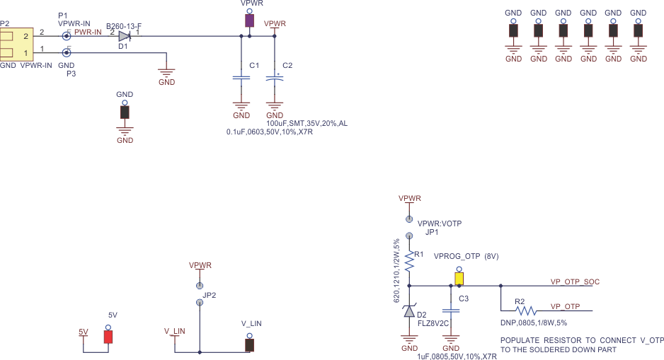
schematic_power_sdu007.gifFigure 19. Schematic, Power
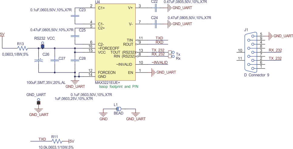
schematic_RS232_sdu007.gifFigure 20. Schematic, RS232

spacer

spacer
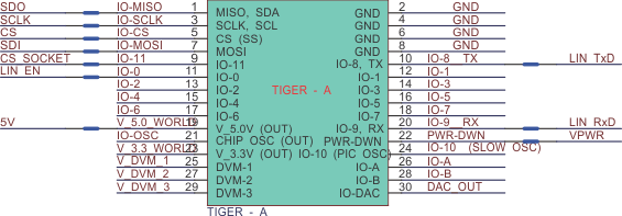
schematic_USB_sdu007.gifFigure 21. Schematic, USB Controller
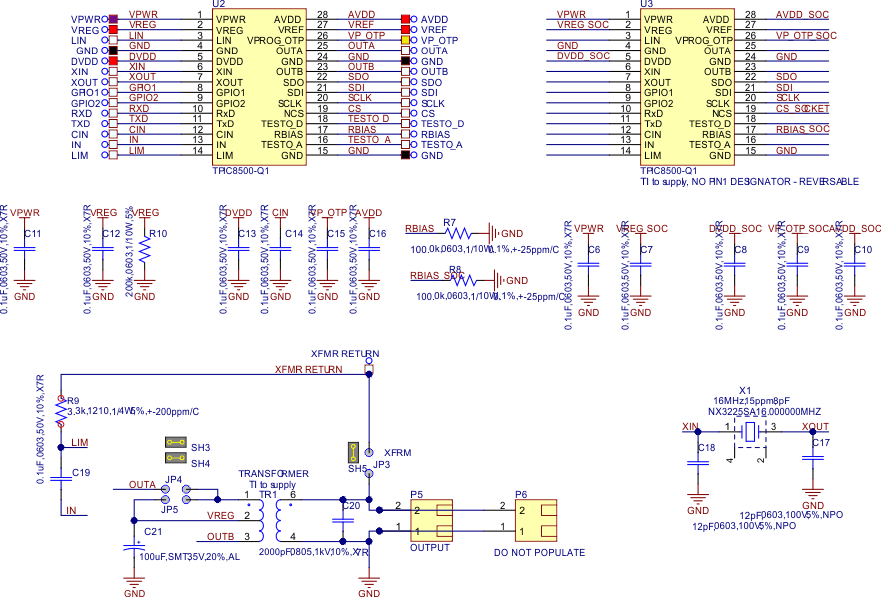
schematic_PGA450_sdu007.gif
C20 is a temperature compensation capacitor for the XDCR. Match C20 to the selected XDCR. If XDCR is Murata MA58MF14-7N, 2000-pF capacitance is installed, and 1500-pF capacitance is provided as an alternative. If XDCR is Murata MA58AF14-0N. 1500-pF capacitance is installed. Alternative specifications include: 1500 pF, 0805, 250 V, 20%, NPO
Figure 22. Schematic, PGA450-Q1 (TPIC8500-Q1)
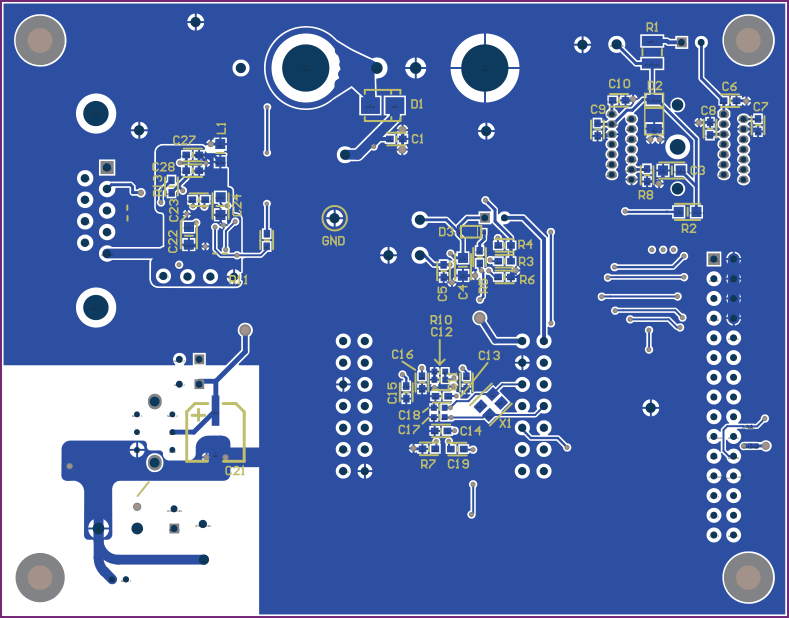
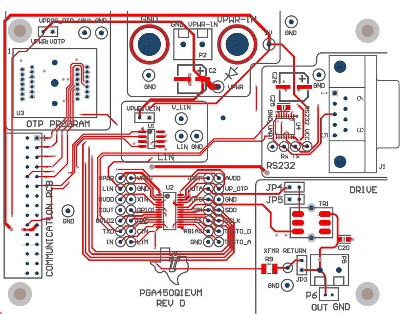
PCB_bottom_sdu007.gifFigure 23. PCB Layout, Bottom
PCB_top_sdu007.gifFigure 24. PCB Layout, Top