SLDU007C March 2012 – November 2015 PGA450-Q1
-
PGA450Q1EVM User’s Guide
- Trademarks
- 1 Read This First
- 2 EVM Overview
- 3 Power-Supply Requirements and Connections
- 4 Jumper Settings
- 5 Socket for Programming OTP
- 6 Transformer and Transducer
- 7 PGA450-Q1 Communication Interfaces
- 8 Controlling the PGA450-Q1 Memory Spaces With the GUI
- 9 LIN Master
- 10 Keil uVision Settings for Programming Firmware to the PGA450-Q1 DEVRAM or OTP Memory
- 11 Use Case
- 12 PGA450Q1EVM Schematics and Layout Drawings
- Revision History
10.2 Setup
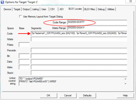
 Figure 11. DEVRAM Target Options
 To Program to DEVRAM:
- Change the code range to the DEVRAM memory space.
- Right click on Target 1 in the project window, and select Options for Target.
- Go to the BL51 Locate tab, and modify the Code Range to go from 0x2000–0x3FFF.
- Copy the following to the Code box:
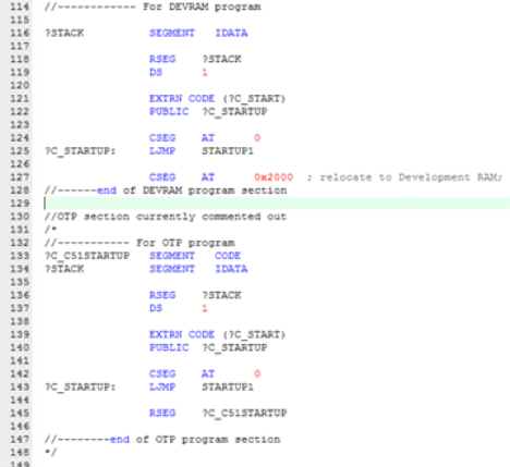
- Comment out the OTP section in STARTUP.A51, and uncomment the OTP section
- An example of this is shown in Figure 13.
?pr?external1_ISR?PGA450_isrs (0X2100),
?pr?timer0_ISR?PGA450_isrs (0X2400),
?pr?timer1_ISR?PGA450_isrs (0X2800),
?pr?serial_ISR?PGA450_isrs (0X2C00),
?pr?linPID_ISR?PGA450_isrs (0X3000),
?pr?linSciRxData_ISR?PGA450_isrs (0X3400),
?pr?linSciTxData_ISR?PGA450_isrs (0X3800),
?pr?external0_ISR?PGA450_isrs (0X3900),
?pr?linSync_ISR?PGA450_isrs (0X3D00)
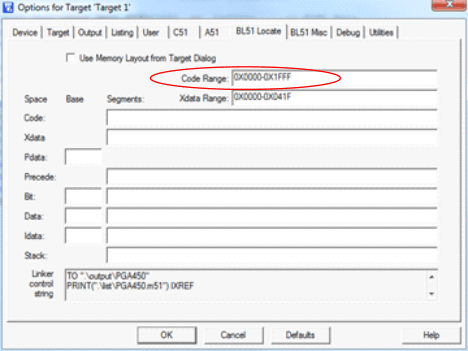
 Figure 12. OTP Target Options
 To Program to OTP:
- Change the code range to the OTP memory space
- Right click on Target 1 in the project window, and select Options for Target.
- Go to the BL51 Locate tab, and modify the Code Range to go from 0x0000–0x1FFF.
- Delete everything in the Code box.
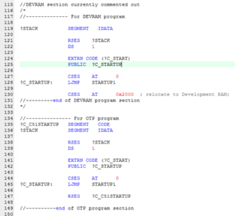
- Comment out the DEVRAM section in STARTUP.A51, and uncomment the OTP section.
- An example of this is shown in Figure 14.
 Figure 13. DEVRAM STARTUP.A51 Example
  Figure 14. OTP STARTUP.A51 Example
 Instructions: Build the PGA450.uvproj to generate the custom .HEX file used to program the internal 8051 core. The LIN Demonstration using PGA450Q1EVM Firmware Rev 2.1 provides instructions on how to upload the .HEX file using the EVM GUI.