SLLA530 December 2020 TCAN1145-Q1
4 Pin Failure Mode Analysis (Pin FMA)
This section provides a Failure Mode Analysis (FMA) for the pins of the TCAN1145-Q1. The failure modes covered in this document include the typical pin-by-pin failure scenarios:
- Pin short-circuited to Ground (see Table 4-2)
- Pin open-circuited (see Table 4-3)
- Pin short-circuited to an adjacent pin (see Table 4-4)
- Pin short-circuited to VSUP (see Table 4-5)
- Pin short-circuited to VCC (see Table 4-6)
- Pin short-circuited to VIO (see Table 4-7)
Table 4-2 through Table 4-7 also indicate how these pin conditions can affect the device as per the failure effects classification in Table 4-1.
| Class | Failure Effects |
|---|---|
| A | Potential device damage that affects functionality |
| B | No device damage, but loss of functionality |
| C | No device damage, but performance degradation |
| D | No device damage, no impact to functionality or performance |
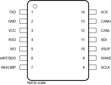
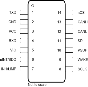
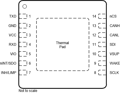
Figure 4-1 shows the TCAN114x-Q1 pin diagrams. For TCAN1145-Q1 pin 6 only supports SDO output and pin 7 only supports INH output. For a detailed description of the device pins please refer to the Pin Configuration and Functions section in the TCAN114x-Q1 data sheet.
 Figure 4-1 14-pin SOIC (D) Pin Diagram, Top
View
 Figure 4-3 14-pin SOT (DYY) Pin Diagram, Top
View.
  Figure 4-2 14-pin VSON (DMT) Pin Diagram, Top
View.
 Following are the assumptions of use and the device configuration assumed for the pin FMA in this section:
- All conditions are within recommended operating conditions
- VSUP = see recommended conditions in device data sheet
- VCC = 4.5 V to 5.5 V
- VIO = 1.71 V to 5.5 V
| Pin Name | Pin No. | Description of Potential Failure Effect(s) | Failure Effect Class |
|---|---|---|---|
| TXD | 1 | Device will enter dominant time out mode. Unable to transmit data from processor to CAN bus | B |
| GND | 2 | None | D |
| VCC | 3 | Transceiver unpowered, high ICC current | B |
| RXD | 4 | Transceiver output biased dominant. Unable to send data from CAN bus to processor | B |
| VIO | 5 | Digital pins unpowered, high IIO current. No communiation between device and processor possible | B |
| SDO | 6 | SDO biased low, no SPI read capability from device to processor | B |
| INH | 7 | INH will not function, excessive VSUP current and not able to perform power enable function | B |
| SCLK | 8 | SCLK biased low, no SPI read/write capability between device and processor | B |
| WAKE | 9 | Will not be able to transition to high, which will not allow device to recognize a local wake up function | B |
| VSUP | 10 | Device unpowered, high ISUP current. | B |
| SDI | 11 | SDI biased low, no SPI write capability from processor to device | B |
| CANL | 12 | VO(REC) spec violated. Degrade EMC performance | B |
| CANH | 13 | Device cannot drive dominant to the bus, no communication possible | B |
| nCS | 14 | nCS biased low, SPI always active | D |
The VSON (DMT) package includes a thermal pad that may or may not be soldered to GND.
| Pin Name | Pin No. | Description of Potential Failure Effect(s) | Failure Effect Class |
|---|---|---|---|
| TXD | 1 | Unable to transmit data from processor to CAN bus | B |
| GND | 2 | Device is unpowered | B |
| VCC | 3 | Transceiver unpowered | B |
| RXD | 4 | Unable to send data from CAN bus to processor | B |
| VIO | 5 | Digital pins unpowered. No communication between device and processor possible | B |
| SDO | 6 | SDO internally biased to VIO. No SPI read capability from device to processor | B |
| INH | 7 | INH will not able to perform system power enable function | B |
| SCLK | 8 | SCLK internally biased to VIO. No SPI read/write capability between device and processor | B |
| WAKE | 9 | Will not be able to transition, which will not allow device to recognize a local wake up function | B |
| VSUP | 10 | Device unpowered | B |
| SDI | 11 | SDI internally biased to VIO. No SPI write capability from processor to device | B |
| CANL | 12 | Device cannot drive dominant to the bus, unable to communicate | B |
| CANH | 13 | Device cannot drive dominant to the bus, unable to communicate | B |
| nCS | 14 | nCS internally biased to VIO. No SPI read/write capability between device and processor | B |
| Pin Name | Pin No. | Shorted to | Description of Potential Failure Effect(s) | Failure Effect Class |
|---|---|---|---|---|
| TXD | 1 | GND | Device will enter dominant time out mode. Unable to transmit data from processor to CAN bus | B |
| GND | 2 | VCC | Device unpowered, high ICC current | B |
| VCC | 3 | RXD | RXD output biased recessive, unable to communicate bus data to processor. | B |
| RXD | 4 | VIO | RXD output biased recessive, unable to communicate bus data to processor. | B |
| VIO | 5 | SDO | No SPI read capability from device to processor | B |
| SDO | 6 | INH | SDO pin will be damaged due to high voltage | A |
| SCLK | 8 | WAKE | SCLK pin may be damaged if WAKE pin connected to VSUP | A |
| WAKE | 9 | VSUP | Will not be able to transition to low, which will not allow device to recognize a local wake up function | B |
| VSUP | 10 | SDI | SDI pin will be damaged and no SPI write communication from processor to device | A |
| SDI | 11 | CANL | SPI SDI bus line will toggle on and off based upon CAN traffic. During SPI communication CANL may toggle due to SDI traffic | B |
| CANL | 12 | CANH | Bus biased recessive, not communication possible. IOS current may be reached on CANH/CANL | B |
| CANH | 13 | nCS | During SPI communication CANH may be biased dominant | B |
There is a chance the thermal pad if soldered down could short to any pin on device. What the thermal pad is soldered to determines the behavior.
Example: if soldered to a ground plane then the adjacent pins would behave as if shorted to ground.
| Pin Name | Pin No. | Description of Potential Failure Effect(s) | Failure Effect Class |
|---|---|---|---|
| TXD | 1 | Absolute maximum violation, pin may be damaged. Unable to communicate from processor to CAN bus | A |
| GND | 2 | Device unpowered, high ISUP current, may damage device | A |
| VCC | 3 | Absolute maximum violation, pin may be damaged. Unable to communicate from processor to CAN bus | A |
| RXD | 4 | Absolute maximum violation, pin may be damaged. Unable to communicate from CAN bus to processor | A |
| VIO | 5 | Absolute maximum violation, pin may be damaged | A |
| SDO | 6 | Absolute maximum violation, pin may be damaged. No SPI read capability from device to processor | A |
| INH | 7 | INH will be biased on and will not be able to turn off | B |
| SCLK | 8 | Absolute maximum violation, pin may be damaged. No SPI read/write capability between device and processor | A |
| WAKE | 9 | Will not be able to transition which will not allow device to recognize a local wake up function | B |
| VSUP | 10 | None | D |
| SDI | 11 | Absolute maximum violation, pin may be damaged, no SPI write capability from processor to device | A |
| CANL | 12 | RXD biased recessive, no communication from CAN bus to processor possible. IOS current may be reached | B |
| CANH | 13 | VO(REC) spec violated. May degrade EMC performance | C |
| nCS | 14 | Absolute maximum violation, transceiver may be damaged. No SPI read/write capability between device and processor | A |
| Pin Name | Pin No. | Description of Potential Failure Effect(s) | Failure Effect Class |
|---|---|---|---|
| TXD | 1 | TXD biased recessive. Unable to transmit data from processor to CAN bus. Processor may be damaged if VCC > VIO | B |
| GND | 2 | Device unpowered, high ICC current | B |
| VCC | 3 | None | D |
| RXD | 4 | Transceiver output biased recessive. Unable to send data from CAN bus to processor. Processor may be damaged if VCC > VIO | B |
| VIO | 5 | IO pins will operate as 5V input/outputs. Processor may be damaged if VCC > VIO | C |
| SDO | 6 | No SPI read capability from device to processor. Processor may be damaged if VCC > VIO | B |
| INH | 7 | May damage transceiver as absolute maximum voltage on VCC may be exceeded | A |
| SCLK | 8 | No SPI read/write capability between device and processor. Processor may be damaged if VCC > VIO | B |
| WAKE | 9 | May damage transceiver as absolute maximum voltage on VCC may be exceeded. May not be able to transition states which will not allow device to recognize a local wake up function | A |
| VSUP | 10 | Absolute maximum violation on VCC, transceiver may be damaged. Unable to communicate from processor to CAN bus | A |
| SDI | 11 | No SPI write capability from processor to device. Processor may be damaged if VCC > VIO | B |
| CANL | 12 | RXD always recessive, no communication possible. IOS current may be reached | B |
| CANH | 13 | VO(REC) spec violated, degraded EMC performance. | C |
| nCS | 14 | No SPI read/write capability between device and processor. Processor may be damaged if VCC > VIO | B |
| Pin Name | Pin No. | Description of Potential Failure Effect(s) | Failure Effect Class |
|---|---|---|---|
| TXD | 1 | TXD biased recessive. Unable to transmit data from processor to CAN bus | B |
| GND | 2 | Device unpowered, high IIO current | B |
| VCC | 3 | IO pins will operate as 5V input/outputs. Processor may be damaged if VCC > VIO. | C |
| RXD | 4 | Transceiver output biased recessive. Unable to send data from CAN bus to processor | B |
| VIO | 5 | None | D |
| SDO | 6 | No SPI read capability from device to processor | B |
| INH | 7 | May damage transceiver as absolute maximum voltage on VIO may be exceeded | A |
| SCLK | 8 | SCLK biased high. No SPI read/write capability between device and processor | B |
| WAKE | 9 | May damage transceiver as absolute maximum voltage on VIO may be exceeded. May not be able to transition states which will not allow device to recognize a local wake up function | A |
| VSUP | 10 | Absolute maximum violation on VIO pin, transceiver may be damaged | A |
| SDI | 11 | SDI biased high. No SPI write capability from processor to device | B |
| CANL | 12 | RXD biased recessive, no communication from bus to processor. IOS current may be reached if VIO ≥ 3.3V. | B |
| CANH | 13 | VO(REC) spec violated. May degrade EMC performance | C |
| nCS | 14 | nCS biased high. No SPI read/write capability between device and processor | B |