SLLSE75B May 2011 – July 2016 TLK10002
PRODUCTION DATA.
- 1 Features
- 2 Applications
- 3 Description
- 4 Revision History
- 5 Description (continued)
- 6 Pin Configuration and Functions
-
7 Specifications
- 7.1 Absolute Maximum Ratings
- 7.2 ESD Ratings
- 7.3 Recommended Operating Conditions
- 7.4 Thermal Information
- 7.5 10-Gbps Power Characteristics - 1.0 V
- 7.6 10-Gbps Power Characteristics - 1.5 V
- 7.7 10-Gbps Power Characteristics - 1.8 V
- 7.8 Transmitter and Receiver Characteristics
- 7.9 MDIO Timing Requirements
- 7.10 JTAG Timing Requirements
- 7.11 Typical Characteristics
-
8 Detailed Description
- 8.1 Overview
- 8.2 Functional Block Diagram
- 8.3
Feature Description
- 8.3.1 High-Speed Side Receiver Jitter Tolerance
- 8.3.2 Lane Alignment Scheme
- 8.3.3 Lane Alignment Components
- 8.3.4 Lane Alignment Operation
- 8.3.5 Channel Synchronization
- 8.3.6 Line Rate, SERDES PLL Settings, and Reference Clock Selection
- 8.3.7 Clocking Architecture
- 8.3.8 Loopback Modes
- 8.3.9 Deep Remote Loopback
- 8.3.10 Shallow Remote Loopback and Serial Retime
- 8.3.11 Deep Local Loopback
- 8.3.12 Shallow Local Loopback
- 8.3.13 Test Pattern Generation and Verification
- 8.3.14 Latency Measurement Function
- 8.3.15 Power-Down Mode
- 8.3.16 High Speed CML Output
- 8.3.17 High Speed Receiver
- 8.3.18 Loss of Signal Indication (LOS)
- 8.3.19 MDIO Management Interface
- 8.3.20 MDIO Protocol Timing
- 8.3.21 Clause 22 Indirect Addressing
- 8.4 Device Functional Modes
- 8.5 Programming
- 8.6 Register Maps
- 9 Application and Implementation
- 10Power Supply Recommendations
- 11Layout
- 12Device and Documentation Support
- 13Mechanical, Packaging, and Orderable Information
7 Specifications
7.1 Absolute Maximum Ratings
over operating free-air temperature range (unless otherwise noted)(1)| MIN | MAX | UNIT | ||
|---|---|---|---|---|
| Supply voltage | DVDD, VDDA_LS/HS, VDDT_LS/HS, VPP, VDDD | –0.3 | 1.4 | V |
| Supply voltage | VDDRA_LS/HS, VDDRB_LS/HS, VDDO[1:0] | –0.3 | 2.2 | V |
| Input voltage | VI, (LVCMOS/LVDS/LVPECL/CML/Analog) | –0.3 | Supply + 0.3 | V |
| Characterized free-air operating temperature | –40 | 85 | °C | |
| Storage temperature, Tstg | –65 | 150 | °C | |
(1) Stresses beyond those listed under Absolute Maximum Ratings may cause permanent damage to the device. These are stress ratings only, which do not imply functional operation of the device at these or any other conditions beyond those indicated under Recommended Operating Conditions. Exposure to absolute-maximum-rated conditions for extended periods may affect device reliability.
7.2 ESD Ratings
| VALUE | UNIT | |||
|---|---|---|---|---|
| V(ESD) | Electrostatic discharge | Human-body model (HBM), per ANSI/ESDA/JEDEC JS-001(1) | ±1000 | V |
| Charged-device model (CDM), per JEDEC specification JESD22-C101(2) | ±500 | |||
(1) JEDEC document JEP155 states that 500-V HBM allows safe manufacturing with a standard ESD control process.
(2) JEDEC document JEP157 states that 250-V CDM allows safe manufacturing with a standard ESD control process.
7.3 Recommended Operating Conditions
| MIN | NOM | MAX | UNIT | |||||
|---|---|---|---|---|---|---|---|---|
| Digital / Analog supply voltages | VDDD, VDDA_LS/HS, DVDD, VDDT_LS/HS, VPP | 0.95 | 1.00 | 1.05 | V | |||
| SERDES PLL regulator voltage | VDDRA_LS/HS VDDRB_LS/HS |
1.5 V nominal | 1.425 | 1.5 | 1.575 | V | ||
| 1.8 V nominal | 1.71 | 1.8 | 1.89 | V | ||||
| LVCMOS I/O supply voltage | VDDO[1:0] | 1.5 V nominal | 1.425 | 1.5 | 1.575 | V | ||
| 1.8 V nominal | 1.71 | 1.8 | 1.89 | V | ||||
| IDD | Supply current | VDDD | 10 Gbps | 375 | mA | |||
| VDDA_LS/HS | 460 | |||||||
| DVDD + VPP | 220 | |||||||
| VDDT_LS/HS | 540 | |||||||
| VDDRA_LS | 50 | |||||||
| VDDRA_HS | 20 | |||||||
| VDDRB_LS | 50 | |||||||
| VDDRB_HS | 20 | |||||||
| VDDO[1:0] (1.5-V /1.8-V Mode) | 1.5-V mode | 6 | ||||||
| 1.8-V mode | 8 | |||||||
| PD | All supplies worst case | 1.75(1) | W | |||||
| ISD | Shutdown current | VDDD | PD* Asserted | 80 | mA | |||
| VDDA | 25 | |||||||
| DVDD + VPP | 15 | |||||||
| VDDT | 45 | |||||||
| VDDRA_HS/LS + VDDRB_HS/LS | 1.5-V mode | 0.5 | ||||||
| 1.8-V mode | 0.5 | |||||||
| VDDO | 1.5-V mode | 5 | ||||||
| 1.8-V mode | 5 | |||||||
(1) Total worst case power is not a sum of the individual power supply worst case as the individual power is taken from multiple modes. These modes are mutually exclusive and therefore used only for power supply requirements.
7.4 Thermal Information
| THERMAL METRIC(1) | TLK10002 | UNIT | ||
|---|---|---|---|---|
| CTR (FCBGA) | ||||
| 144 PINS | ||||
| RθJA | Junction-to-ambient thermal resistance | 24.5 | °C/W | |
| EVM Board (5in. x 7in., 14 layer, 1-oz. copper) | 24.5 | |||
| JEDEC High-K PCB | 25.5 | |||
| RθJC(top) | Junction-to-case (top) thermal resistance | SPACE | 2.8 | °C/W |
| EVM Board (5in. x 7in., 14 layer, 1-oz. copper) | ||||
| JEDEC High-K PCB | ||||
| RθJB | Junction-to-board thermal resistance | 15.2 | °C/W | |
| EVM Board (5in. x 7in., 14 layer, 1-oz. copper) | 12 | |||
| JEDEC High-K PCB | 18 | |||
| ψJT | Junction-to-top characterization parameter | 0.9 | °C/W | |
| EVM Board (5in. x 7in., 14 layer, 1-oz. copper) | 0.9 | |||
| JEDEC High-K PCB | 1.8 | |||
| ψJB | Junction-to-board characterization parameter | 14.0 | °C/W | |
| EVM Board (5in. x 7in., 14 layer, 1-oz. copper) | 11 | |||
| JEDEC High-K PCB | 13.7 | |||
| RθJC(bot) | Junction-to-case (bottom) thermal resistance | — | °C/W | |
(1) For more information about traditional and new thermal metrics, see the Semiconductor and IC Package Thermal Metrics application report.
7.5 10-Gbps Power Characteristics – 1.0 V
at Vmax, 1.0 V Core, over operating free-air temperature range (unless otherwise noted)| PARAMETER | TEST CONDITIONS | MIN | TYP | MAX | UNIT | ||
|---|---|---|---|---|---|---|---|
| Power supply voltage | VDDA_LS/HS, VDDT_LS/HS, VDDD, DVDD, VPP | 2 Ch Mode, 4:1 at 10 Gpbs | 0.95 | 1 | 1.05 | V | |
| 2 Ch Mode, 2:1 at 10 Gpbs | |||||||
| 1 Ch Mode, Ch A on, Ch B off, 4:1 at 10 Gpbs | |||||||
| 1 Ch Mode, Ch A on, Ch B off, 2:1 at 10 Gpbs | |||||||
| 1 Ch Mode, Ch A off, Ch B on, 4:1 at 10 Gpbs | |||||||
| 1 Ch Mode, Ch A off, Ch B on, 2:1 at 10 Gpbs | |||||||
| Power supply current | VDDA_LS/HS | 2 Ch Mode, 4:1 at 10 Gpbs | 0.407 | A | |||
| 2 Ch Mode, 2:1 at 10 Gpbs | 0.411 | ||||||
| 1 Ch Mode, Ch A on, Ch B off, 4:1 at 10 Gpbs | 0.222 | ||||||
| 1 Ch Mode, Ch A on, Ch B off, 2:1 at 10 Gpbs | 0.22 | ||||||
| 1 Ch Mode, Ch A off, Ch B on, 4:1 at 10 Gpbs | 0.229 | ||||||
| 1 Ch Mode, Ch A off, Ch B on, 2:1 at 10 Gpbs | 0.228 | ||||||
| VDDT_LS/HS | 2 Ch Mode, 4:1 at 10 Gpbs | 0.489 | A | ||||
| 2 Ch Mode, 2:1 at 10 Gpbs | 0.347 | ||||||
| 1 Ch Mode, Ch A on, Ch B off, 4:1 at 10 Gpbs | 0.268 | ||||||
| 1 Ch Mode, Ch A on, Ch B off, 2:1 at 10 Gpbs | 0.197 | ||||||
| 1 Ch Mode, Ch A off, Ch B on, 4:1 at 10 Gpbs | 0.273 | ||||||
| 1 Ch Mode, Ch A off, Ch B on, 2:1 at 10 Gpbs | 0.199 | ||||||
| DVDD+VPP | 2 Ch Mode, 4:1 at 10 Gpbs | 0.1743 | A | ||||
| 2 Ch Mode, 2:1 at 10 Gpbs | 0.1887 | ||||||
| 1 Ch Mode, Ch A on, Ch B off, 4:1 at 10 Gpbs | 0.1375 | ||||||
| 1 Ch Mode, Ch A on, Ch B off, 2:1 at 10 Gpbs | 0.1407 | ||||||
| 1 Ch Mode, Ch A off, Ch B on, 4:1 at 10 Gpbs | 0.1356 | ||||||
| 1 Ch Mode, Ch A off, Ch B on, 2:1 at 10 Gpbs | 0.1414 | ||||||
| VDDD | 2 Ch Mode, 4:1 at 10 Gpbs | 0.3151 | A | ||||
| 2 Ch Mode, 2:1 at 10 Gpbs | 0.333 | ||||||
| 1 Ch Mode, Ch A on, Ch B off, 4:1 at 10 Gpbs | 0.21 | ||||||
| 1 Ch Mode, Ch A on, Ch B off, 2:1 at 10 Gpbs | 0.2136 | ||||||
| 1 Ch Mode, Ch A off, Ch B on, 4:1 at 10 Gpbs | 0.209 | ||||||
| 1 Ch Mode, Ch A off, Ch B on, 2:1 at 10 Gpbs | 0.2165 | ||||||
7.6 10-Gbps Power Characteristics – 1.5 V
at Vmax, 1.5 V I/O, over operating free-air temperature range (unless otherwise noted)| PARAMETER | TEST CONDITIONS | MIN | TYP | MAX | UNIT | ||
|---|---|---|---|---|---|---|---|
| Power supply voltage | VDDRA_LS/HS, VDDRB_LS/HS, VDDO | 2 Ch Mode, 4:1 at 10 Gpbs | 1.425 | 1.5 | 1.575 | V | |
| 2 Ch Mode, 2:1 at 10 Gpbs | |||||||
| 1 Ch Mode, Ch A on, Ch B off, 4:1 at 10 Gpbs | |||||||
| 1 Ch Mode, Ch A on, Ch B off, 2:1 at 10 Gpbs | |||||||
| 1 Ch Mode, Ch A off, Ch B on, 4:1 at 10 Gpbs | |||||||
| 1 Ch Mode, Ch A off, Ch B on, 2:1 at 10 Gpbs | |||||||
| Power supply current | VDDRA_LS | 2 Ch Mode, 4:1 at 10 Gpbs | 0.0191 | A | |||
| 2 Ch Mode, 2:1 at 10 Gpbs | 0.0371 | ||||||
| 1 Ch Mode, Ch A on, Ch B off, 4:1 at 10 Gpbs | 0.019 | ||||||
| 1 Ch Mode, Ch A on, Ch B off, 2:1 at 10 Gpbs | 0.0371 | ||||||
| 1 Ch Mode, Ch A off, Ch B on, 4:1 at 10 Gpbs | 0 | ||||||
| 1 Ch Mode, Ch A off, Ch B on, 2:1 at 10 Gpbs | 0 | ||||||
| VDDRA_HS | 2 Ch Mode, 4:1 at 10 Gpbs | 0.0152 | A | ||||
| 2 Ch Mode, 2:1 at 10 Gpbs | 0.0152 | ||||||
| 1 Ch Mode, Ch A on, Ch B off, 4:1 at 10 Gpbs | 0.0153 | ||||||
| 1 Ch Mode, Ch A on, Ch B off, 2:1 at 10 Gpbs | 0.0153 | ||||||
| 1 Ch Mode, Ch A off, Ch B on, 4:1 at 10 Gpbs | 0 | ||||||
| 1 Ch Mode, Ch A off, Ch B on, 2:1 at 10 Gpbs | 0 | ||||||
| VDDRB_LS | 2 Ch Mode, 4:1 at 10 Gpbs | 0.0192 | A | ||||
| 2 Ch Mode, 2:1 at 10 Gpbs | 0.0374 | ||||||
| 1 Ch Mode, Ch A on, Ch B off, 4:1 at 10 Gpbs | 0 | ||||||
| 1 Ch Mode, Ch A on, Ch B off, 2:1 at 10 Gpbs | 0 | ||||||
| 1 Ch Mode, Ch A off, Ch B on, 4:1 at 10 Gpbs | 0.0192 | ||||||
| 1 Ch Mode, Ch A off, Ch B on, 2:1 at 10 Gpbs | 0.0374 | ||||||
| VDDRB_HS | 2 Ch Mode, 4:1 at 10 Gpbs | 0.0155 | A | ||||
| 2 Ch Mode, 2:1 at 10 Gpbs | 0.0155 | ||||||
| 1 Ch Mode, Ch A on, Ch B off, 4:1 at 10 Gpbs | 0 | ||||||
| 1 Ch Mode, Ch A on, Ch B off, 2:1 at 10 Gpbs | 0 | ||||||
| 1 Ch Mode, Ch A off, Ch B on, 4:1 at 10 Gpbs | 0.0156 | ||||||
| 1 Ch Mode, Ch A off, Ch B on, 2:1 at 10 Gpbs | 0.0156 | ||||||
| VDDO[1:0] | 2 Ch Mode, 4:1 at 10 Gpbs | 0.0037 | A | ||||
| 2 Ch Mode, 2:1 at 10 Gpbs | |||||||
| 1 Ch Mode, Ch A on, Ch B off, 4:1 at 10 Gpbs | |||||||
| 1 Ch Mode, Ch A on, Ch B off, 2:1 at 10 Gpbs | |||||||
| 1 Ch Mode, Ch A off, Ch B on, 4:1 at 10 Gpbs | |||||||
| 1 Ch Mode, Ch A off, Ch B on, 2:1 at 10 Gpbs | |||||||
7.7 10-Gbps Power Characteristics – 1.8 V
at Vmax, 1.8 V I/O, over operating free-air temperature range (unless otherwise noted)| PARAMETER | TEST CONDITIONS | MIN | TYP | MAX | UNIT | ||
|---|---|---|---|---|---|---|---|
| Power supply voltage | VDDRA_LS/HS, VDDRB_LS/HS, VDDO | 2 Ch Mode, 4:1 at 10 Gpbs | 1.71 | 1.8 | 1.89 | V | |
| 2 Ch Mode, 2:1 at 10 Gpbs | |||||||
| 1 Ch Mode, Ch A on, Ch B off, 4:1 at 10 Gpbs | |||||||
| 1 Ch Mode, Ch A on, Ch B off, 2:1 at 10 Gpbs | |||||||
| 1 Ch Mode, Ch A off, Ch B on, 4:1 at 10 Gpbs | |||||||
| 1 Ch Mode, Ch A off, Ch B on, 2:1 at 10 Gpbs | |||||||
| Power supply current | VDDRA_LS | 2 Ch Mode, 4:1 at 10 Gpbs | 0.0191 | A | |||
| 2 Ch Mode, 2:1 at 10 Gpbs | 0.0372 | ||||||
| 1 Ch Mode, Ch A on, Ch B off, 4:1 at 10 Gpbs | 0.0191 | ||||||
| 1 Ch Mode, Ch A on, Ch B off, 2:1 at 10 Gpbs | 0.0372 | ||||||
| 1 Ch Mode, Ch A off, Ch B on, 4:1 at 10 Gpbs | 0 | ||||||
| 1 Ch Mode, Ch A off, Ch B on, 2:1 at 10 Gpbs | 0 | ||||||
| VDDRA_HS | 2 Ch Mode, 4:1 at 10 Gpbs | 0.0151 | A | ||||
| 2 Ch Mode, 2:1 at 10 Gpbs | 0.0151 | ||||||
| 1 Ch Mode, Ch A on, Ch B off, 4:1 at 10 Gpbs | 0.0151 | ||||||
| 1 Ch Mode, Ch A on, Ch B off, 2:1 at 10 Gpbs | 0.0151 | ||||||
| 1 Ch Mode, Ch A off, Ch B on, 4:1 at 10 Gpbs | 0 | ||||||
| 1 Ch Mode, Ch A off, Ch B on, 2:1 at 10 Gpbs | 0 | ||||||
| VDDRB_LS | 2 Ch Mode, 4:1 at 10 Gpbs | 0.0194 | A | ||||
| 2 Ch Mode, 2:1 at 10 Gpbs | 0.0376 | ||||||
| 1 Ch Mode, Ch A on, Ch B off, 4:1 at 10 Gpbs | 0 | ||||||
| 1 Ch Mode, Ch A on, Ch B off, 2:1 at 10 Gpbs | 0 | ||||||
| 1 Ch Mode, Ch A off, Ch B on, 4:1 at 10 Gpbs | 0.0193 | ||||||
| 1 Ch Mode, Ch A off, Ch B on, 2:1 at 10 Gpbs | 0.0376 | ||||||
| VDDRB_HS | 2 Ch Mode, 4:1 at 10 Gpbs | 0.0154 | A | ||||
| 2 Ch Mode, 2:1 at 10 Gpbs | 0.0154 | ||||||
| 1 Ch Mode, Ch A on, Ch B off, 4:1 at 10 Gpbs | 0 | ||||||
| 1 Ch Mode, Ch A on, Ch B off, 2:1 at 10 Gpbs | 0 | ||||||
| 1 Ch Mode, Ch A off, Ch B on, 4:1 at 10 Gpbs | 0.0155 | ||||||
| 1 Ch Mode, Ch A off, Ch B on, 2:1 at 10 Gpbs | 0.0155 | ||||||
| VDDO[1:0] | 2 Ch Mode, 4:1 at 10 Gpbs | 0.0047 | A | ||||
| 2 Ch Mode, 2:1 at 10 Gpbs | 0.0047 | ||||||
| 1 Ch Mode, Ch A on, Ch B off, 4:1 at 10 Gpbs | 0.0046 | ||||||
| 1 Ch Mode, Ch A on, Ch B off, 2:1 at 10 Gpbs | 0.0047 | ||||||
| 1 Ch Mode, Ch A off, Ch B on, 4:1 at 10 Gpbs | 0.0046 | ||||||
| 1 Ch Mode, Ch A off, Ch B on, 2:1 at 10 Gpbs | 0.0047 | ||||||
7.8 Transmitter and Receiver Characteristics
| PARAMETER | TEST CONDITIONS | MIN | TYP | MAX | UNIT | |
|---|---|---|---|---|---|---|
| HIGH-SPEED SIDE SERIAL TRANSMITTER | ||||||
| VOD(pp) | TX Output differential peak-to-peak voltage swing | SWING (3.15:12) = 0000 | 50 | 130 | 220 | mVpp |
| SWING (3.15:12) = 0001 | 110 | 220 | 320 | |||
| SWING (3.15:12) = 0010 | 180 | 300 | 430 | |||
| SWING (3.15:12) = 0011 | 250 | 390 | 540 | |||
| SWING (3.15:12) = 0100 | 320 | 480 | 650 | |||
| SWING (3.15:12) = 0101 | 390 | 570 | 770 | |||
| SWING (3.15:12) = 0110 | 460 | 660 | 880 | |||
| SWING (3.15:12) = 0111 | 530 | 750 | 1000 | |||
| SWING (3.15:12) = 1000 | 590 | 830 | 1100 | |||
| SWING (3.15:12) = 1001 | 660 | 930 | 1220 | |||
| SWING (3.15:12) = 1010 | 740 | 1020 | 1320 | |||
| SWING (3.15:12) = 1011 | 820 | 1110 | 1430 | |||
| SWING (3.15:12) = 1100 | 890 | 1180 | 1520 | |||
| SWING (3.15:12) = 1101 | 970 | 1270 | 1610 | |||
| SWING (3.15:12) = 1110 | 1060 | 1340 | 1680 | |||
| SWING (3.15:12) = 1111 | 1090 | 1400 | 1740 | |||
| VCMT | TX Output common-mode voltage | 100-Ω differential termination, DC-coupled | VDDT-(0.25*VOD(pp)) | mV | ||
| tskew | Intra-pair output skew | SWING(3.15:12) = 0110 | 0.09 | UI | ||
| tr, tf | Differential output signal rise, Fall time (20% to 80%) Differential load = 100Ω |
20 | ps | |||
| JT1 | Serial output total jitter (CPRI LV/LV-II/LV-III and OBSAI Rates) | Serial Rate ≤ 3.072 Gbps (Not Applicable to LV-II/LV-III) |
0.35 | UI | ||
| Serial Rate > 3.072 Gbps (And All LV-II/LV-III Rates) |
0.30 | |||||
| JD1 | Serial output deterministic jitter (CPRI LV/LV-II/ LV-III and OBSAI Rates) | Serial Rate ≤ 3.072 Gbps (Not Applicable to LV-II/LV-III) |
0.17 | UI | ||
| Serial Rate > 3.072 Gbps (And All LV-II/LV-III Rates) |
0.15 | |||||
| JT2 | Serial output total jitter (CPRI E.12.HV) |
CPRI E.12.HV (0.6144 and 1.2288 Gbps) | 0.279 | UI | ||
| JD2 | Serial output deterministic jitter (CPRI E.12.HV) | 0.14 | ||||
| Scc22 | Common-mode output return loss | 100MHz < f < 1.0 GHz | 7 | dB | ||
| 1.0GHz < f < 5.0 GHz | 5 | |||||
| T(LATENCY) | Transmit path latency | See Figure 19 | UI | |||
| HIGH-SPEED SIDER SERIAL RECEIVER | ||||||
| VID | RX Input differential voltage |RXP – RXN| | Full Rate AC-Coupled | 50 | 600 | mV | |
| Half/Quarter/Eighth Rate AC-Coupled | 50 | 800 | ||||
| VID(pp) | RX Input differential peak-to-peak voltage swing 2 * |RXP – RXN| |
Full Rate AC-Coupled | 100 | 1200 | mVpp | |
| Half/Quarter/Eighth Rate AC-Coupled | 100 | 1600 | ||||
| CI | RX Input capacitance | 2 | pF | |||
| JTOL | Jitter tolerance, total jitter at serial input (DJ + RJ) (BER 10-15) | Zero crossing Half/Quarter/Eighth Rate | 0.66 | UIpp | ||
| Zero crossing Full Rate | 0.65 | |||||
| JDR | Serial input deterministic jitter (BER 10-15) | Zero crossing Half/Quarter/Eighth Rate | 0.50 | UIpp | ||
| Zero crossing Full Rate | 0.35 | |||||
| SDD11 | Differential input return loss | 100 MHz < f < 0.75*[Serial Bit Rate] | 8 | dB | ||
| 0.75 × [Serial Bit Rate] < f < [Serial Bit Rate] | See (1) | |||||
| tskew | Intra-pair input skew | 0.23 | UI | |||
| t(LATENCY) | Receive path latency | See Figure 19 | UI | |||
| LOW-SPEED SIDE SERIAL TRANSMITTER CHARACTERISTICS | ||||||
| VOD(pp) | Transmitter output differential peak-to-peak voltage swing | SWING (7:14:12) = 000 | 110 | 190 | 280 | mVpp |
| SWING (7:14:12) = 001 | 280 | 380 | 490 | |||
| SWING (7:14:12) = 010 | 420 | 560 | 700 | |||
| SWING (7:14:12) = 011 | 560 | 710 | 870 | |||
| SWING (7:14:12) = 100 | 690 | 850 | 1020 | |||
| SWING (7:14:12) = 101 | 760 | 950 | 1150 | |||
| SWING (7:14:12) = 110 | 800 | 1010 | 1230 | |||
| SWING (7:14:12)= 111 | 830 | 1050 | 1270 | |||
| VCMT | Transmitter output common mode voltage | 100-Ω differential termination, DC-coupled | VDDT - (0.5*VOD(pp)) | mV | ||
| tskew | Intra-pair output skew | 0.045 | UI | |||
| tR, tF | Differential output signal rise, fall time (20% to 80%) Differential Load = 100Ω | 30 | - | - | ps | |
| JT | Serial output total jitter | 0.35 | UI | |||
| JD | Serial output deterministic jitter | 0.17 | UI | |||
| LOW-SPEED SIDE SERIAL RECEIVER CHARACTERISTICS | ||||||
| VID | Receiver input differential voltage| INP – INN| | Full Rate AC-Coupled | 50 | 600 | mV | |
| Half/Quarter Rate AC-Coupled | 50 | 800 | ||||
| VID(pp) | Receiver input differential peak-to-peak voltage swing 2 × |INP – INN| |
Full Rate AC-Coupled | 100 | 1200 | mVdfpp | |
| Half/Quarter Rate AC-Coupled | 100 | 1600 | ||||
| CI | Receiver input capacitance | 2 | pF | |||
| JTOL | Jitter tolerance, total jitter at serial input (DJ + RJ)(BER 10-15) |
Zero crossing Half/Quarter Rate | 0.66 | UIpp | ||
| Zero crossing Full Rate | 0.65 | |||||
| JDR | Serial input deterministic jitter(BER 10-15) | Zero crossing Half/Quarter Rate | 0.50 | UIpp | ||
| Zero crossing Full Rate | 0.35 | |||||
| Sdd11 | Differential input return loss | 625 MHz < f < 2.5 GHz | 8 | dB | ||
| tskew | Intra-pair input skew | 0.23 | UI | |||
| tlane-skew | Lane-to-lane input skew | 30 | UI | |||
| REFERENCE CLOCK CHARACTERISTICS (REFCLK0P/N, REFCLK1P/N) | ||||||
| F | Frequency | 122.88 | 425 | MHz | ||
| FHSoffset | Accuracy | Relative to Nominal HS Serial Data Rate | –100 | 100 | ppm | |
| Relative to Incoming HS Serial Data Rate | –200 | 200 | ||||
| FLSoffset | Accuracy to LS serial data | Synchronous (Multiple/Divide) | 0 | 0 | 0 | ppm |
| DC | Duty cycle | High Time | 45% | 50% | 55% | |
| VID | Differential input voltage | 250 | 2000 | mVpp | ||
| CIN | Input capacitance | 1 | pF | |||
| RIN | Differential input impedance | 100 | Ω | |||
| TRISE | Rise/fall time | 10% to 90% | 50 | 350 | ps | |
| JR | Random jitter | 12 kHz to 20 MHz | 4 | ps-RMS | ||
| DIFFERENTIAL OUTPUT CLOCK CHARACTERISTICS (CLKOUTAP/N, CLKOUTBP/N) | ||||||
| VOD | Differential Output Voltage | Peak to peak | 1000 | 2000 | mVpp | |
| TRISE | Output Rise Time | 10% to 90%, 2pF lumped capacitive load, AC-Coupled | 350 | ps | ||
| RTERM | Output Termination | CLKOUTA/BP/N to DVDD | 40 | 50 | 60 | Ω |
| F | Output Frequency | 0 | 500 | MHz | ||
| LVCMOS ELECTRICAL CHARACTERISTICS (VDDO) | ||||||
| VOH | High-level output voltage | IOH = 2 mA, Driver Enabled (1.8 V) | VDDO – 0.45 | VDDO | V | |
| IOH = 2 mA, Driver Enabled (1.5 V) | 0.75 × VDDO | VDDO | ||||
| VOL | Low-level output voltage | IOL = –2 mA, Driver Enabled (1.8 V) | 0 | 0.45 | V | |
| IOL = –2 mA, Driver Enabled (1.5 V) | 0 | 0.25 × VDDO | ||||
| VIH | High-level input voltage | 0.65 × VDDO | VDDO + 0.3 | V | ||
| VIL | Low-level input voltage | –0.3 | 0.35 × VDDO | V | ||
| IIH, IIL | Low/high input current | Receiver only | ±170 | µA | ||
| IOZ | High-impedance output current | Driver disabled | ±25 | µA | ||
| Driver disabled with pullup or pulldown enabled | ±195 | |||||
| CIN | Input capacitance | 3 | pF | |||
(1) Differential input return loss, SDD11 = 8 – 16.6 log10(f / (0.75 × [Serial Bit Rate])) dB
7.9 MDIO Timing Requirements
over recommended operating conditions (unless otherwise noted)| PARAMETER | TEST CONDITIONS | MIN | TYP | MAX | UNIT | |
|---|---|---|---|---|---|---|
| tperiod | MDC period | See Figure 4 | 100 | ns | ||
| tsetup | MDIO setup to ↑ MDC | See Figure 4 | 10 | ns | ||
| thold | MDIO hold to ↑ MDC | See Figure 4 | 10 | ns | ||
| tvalid | MDIO valid from MDC ↑ | 0 | 40 | ns | ||
7.10 JTAG Timing Requirements
over recommended operating conditions (unless otherwise noted)| PARAMETER | TEST CONDITIONS | MIN | TYP | MAX | UNIT | |
|---|---|---|---|---|---|---|
| tPERIOD | TCK period | See Figure 5 | 66.67 | ns | ||
| tSETUP | TDI/TMS/TRST_N setup to ↑ TCK | See Figure 5 | 3 | ns | ||
| tHOLD | TDI/TMS/TRST_N hold from ↑ TCK | See Figure 5 | 5 | ns | ||
| tVALID | TDO delay from TCK falling | See Figure 5 | 0 | 10 | ns | |
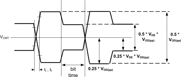 Figure 1. Transmit Output Waveform Parameter Definitions
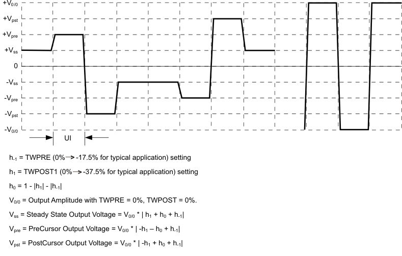 Figure 2. Pre/Post Cursor Swing Definitions
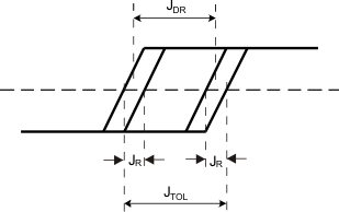
NOTE:
JTOL = JR + JDR, where JTOL is the receive jitter tolerance, JDR is the received deterministic jitter, and JR is the Gaussian random edge jitter distribution at a maximum BER = 10-12 for CPRI link and BER = 10-15 for OBSAI (RP3) link.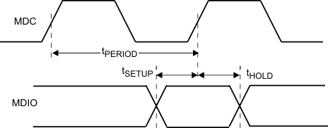 Figure 4. MDIO Read/Write Timing
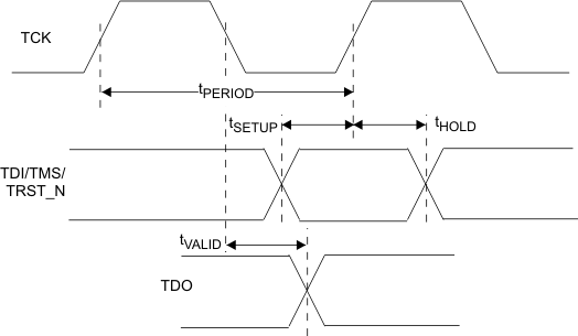 Figure 5. JTAG Timing
7.11 Typical Characteristics
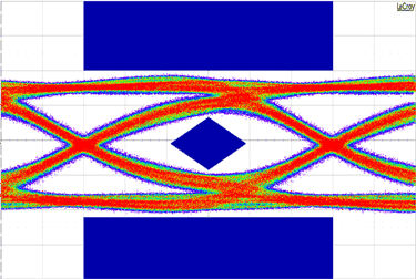
Total Jitter = .298 UI, PRBS 27-1, 4:1 Mode, RefClk=122.88MHz, Swing = 1260 mVpp, PRE = -5, POST1 = -10, POST2 = -7.5, AC-coupled
Figure 6. Transmitter Output (4-Inch FR-4 Trace)
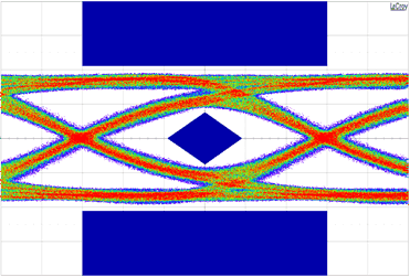
| Total Jitter = .339 UI, PRBS 27-1, 4:1 Mode, RefClk=122.88MHz, Swing = 1260 mVpp, PRE = -2.5, POST1 = -17.5, POST2 = 0, AC-coupled |
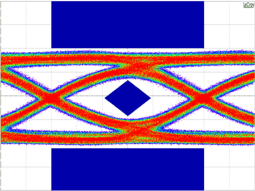
Total Jitter = .339 UI, PRBS 27-1, 4:1 Mode, RefClk=122.88MHz, Swing = 1260 mVpp, PRE = -2.5, POST1 = -17.5, POST2 = 0, AC-coupled
Figure 7. Transmitter Output (8-Inch FR-4 Trace)