SLLSER8J June   2017  – August 2024

PRODUCTION DATA  

  1.   1
  2. Features
  3. Applications
  4. Description
  5. Device Comparison Table
  6. Pin Configuration and Function
  7. Specifications
    1. 6.1  Absolute Maximum Ratings
    2. 6.2  ESD Ratings
    3. 6.3  Recommended Operating Conditions
    4. 6.4  Thermal Information
    5. 6.5  Power Ratings
    6. 6.6  Insulation Specifications for D Package
    7. 6.7  Insulation Specifications for DWV Package
    8. 6.8  Safety-Related Certifications For D Package
    9. 6.9  Safety-Related Certifications For DWV Package
    10. 6.10 Safety Limiting Values
    11. 6.11 Electrical Characteristics
    12. 6.12 Switching Characteristics
    13. 6.13 Insulation Characteristics Curves
    14. 6.14 Typical Characteristics
  8. Parameter Measurement Information
    1. 7.1 Propagation Delay, Inverting, and Noninverting Configuration
      1. 7.1.1 CMTI Testing
  9. Detailed Description
    1. 8.1 Overview
    2. 8.2 Functional Block Diagram
    3. 8.3 Feature Description
      1. 8.3.1 Power Supply
      2. 8.3.2 Input Stage
      3. 8.3.3 Output Stage
      4. 8.3.4 Protection Features
        1. 8.3.4.1 Undervoltage Lockout (UVLO)
        2. 8.3.4.2 Active Pulldown
        3. 8.3.4.3 Short-Circuit Clamping
        4. 8.3.4.4 Active Miller Clamp (UCC53x0M)
    4. 8.4 Device Functional Modes
      1. 8.4.1 ESD Structure
  10. Application and Implementation
    1. 9.1 Application Information
    2. 9.2 Typical Application
      1. 9.2.1 Design Requirements
      2. 9.2.2 Detailed Design Procedure
        1. 9.2.2.1 Designing IN+ and IN– Input Filter
        2. 9.2.2.2 Gate-Driver Output Resistor
        3. 9.2.2.3 Estimate Gate-Driver Power Loss
        4. 9.2.2.4 Estimating Junction Temperature
      3. 9.2.3 Selecting VCC1 and VCC2 Capacitors
        1. 9.2.3.1 Selecting a VCC1 Capacitor
        2. 9.2.3.2 Selecting a VCC2 Capacitor
        3. 9.2.3.3 Application Circuits with Output Stage Negative Bias
      4. 9.2.4 Application Curve
  11. 10Power Supply Recommendations
  12. 11Layout
    1. 11.1 Layout Guidelines
    2. 11.2 Layout Example
    3. 11.3 PCB Material
  13. 12Device and Documentation Support
    1. 12.1 Device Support
      1. 12.1.1 Third-Party Products Disclaimer
    2. 12.2 Documentation Support
      1. 12.2.1 Related Documentation
    3. 12.3 Certifications
    4. 12.4 Receiving Notification of Documentation Updates
    5. 12.5 Support Resources
    6. 12.6 Trademarks
    7. 12.7 Electrostatic Discharge Caution
    8. 12.8 Glossary
  14. 13Revision History
  15. 14Mechanical, Packaging, and Orderable Information

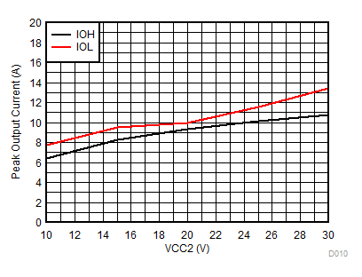
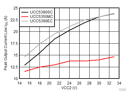
Typical Characteristics

VCC1 = 3.3 V or 5 V, 0.1-µF capacitor from VCC1 to GND1, VCC2= 15 V, 1-µF capacitor from VCC2 to VEE2, CLOAD = 1 nF, TA = –40°C to +125°C, (unless otherwise noted)
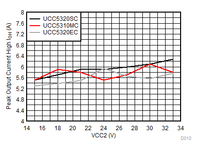
UCC5310 UCC5320 UCC5350 UCC5390 Output-High Drive Current vs Output Voltage
CLOAD = 150 nF
Figure 6-5 Output-High Drive Current vs Output Voltage
UCC5310 UCC5320 UCC5350 UCC5390 UCC5350SBD Output-High Drive Current vs Output Voltage
CLOAD = 150 nF
Figure 6-7 UCC5350SBD Output-High Drive Current vs Output Voltage
UCC5310 UCC5320 UCC5350 UCC5390 Output-Low Drive Current vs Output Voltage
CLOAD = 150 nF
Figure 6-9 Output-Low Drive Current vs Output Voltage
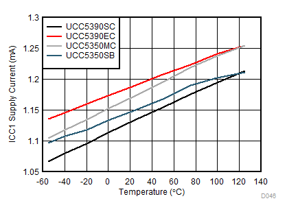
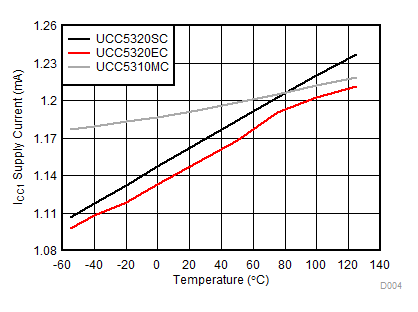
UCC5310 UCC5320 UCC5350 UCC5390 ICC1 Supply Current vs Temperature
IN+ = L IN– = H
Figure 6-11 ICC1 Supply Current vs Temperature
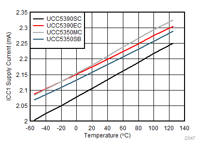
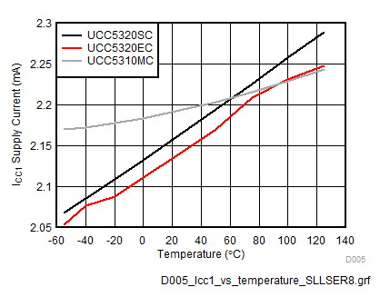
UCC5310 UCC5320 UCC5350 UCC5390 ICC1 Supply Current vs Temperature
IN+ = H IN– = L
Figure 6-13 ICC1 Supply Current vs Temperature
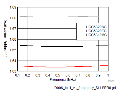
UCC5310 UCC5320 UCC5350 UCC5390 ICC1 Supply Current vs Input Frequency
Duty Cycle = 50% T = 25°C
Figure 6-15 ICC1 Supply Current vs Input Frequency
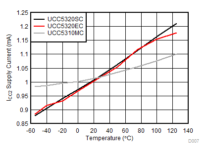
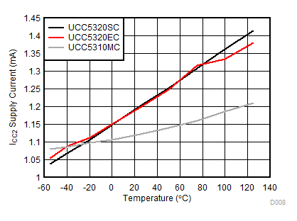
UCC5310 UCC5320 UCC5350 UCC5390 ICC2 Supply Current vs Temperature
IN+ = L IN– = H
Figure 6-17 ICC2 Supply Current vs Temperature
UCC5310 UCC5320 UCC5350 UCC5390 ICC2 Supply Current vs Temperature
IN+ = H IN– = L
Figure 6-19 ICC2 Supply Current vs Temperature
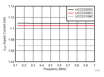
UCC5310 UCC5320 UCC5350 UCC5390 ICC2 Supply Current vs Input Frequency
Duty Cycle = 50% T = 25°C
Figure 6-21 ICC2 Supply Current vs Input Frequency
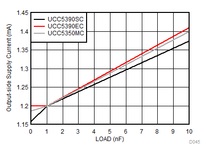
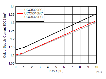
UCC5310 UCC5320 UCC5350 UCC5390 ICC2 Supply Current vs Load Capacitance
fSW = 1 kHz
Figure 6-23 ICC2 Supply Current vs Load Capacitance
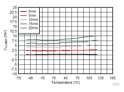
UCC5310 UCC5320 UCC5350 UCC5390 UCC5350M VClamp vs Temperature
IClamp = 0mA~20mA
Figure 6-25 UCC5350M VClamp vs Temperature
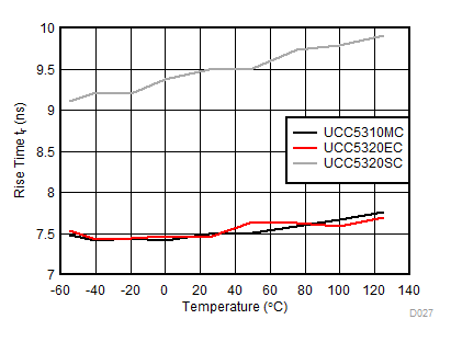
UCC5310 UCC5320 UCC5350 UCC5390 Rise Time vs Temperature
Figure 6-27 Rise Time vs Temperature
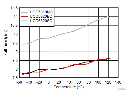
UCC5310 UCC5320 UCC5350 UCC5390 Fall Time Vs Temperature
Figure 6-29 Fall Time Vs Temperature
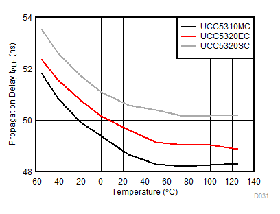
UCC5310 UCC5320 UCC5350 UCC5390 Propagation Delay tPLH vs Temperature
Figure 6-31 Propagation Delay tPLH vs Temperature
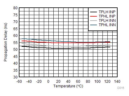
UCC5310 UCC5320 UCC5350 UCC5390 UCC5350SBD Propagation Delay vs Temperature
Figure 6-33 UCC5350SBD Propagation Delay vs Temperature
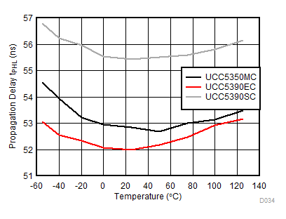
UCC5310 UCC5320 UCC5350 UCC5390 Propagation Delay tPHL vs Temperature
Figure 6-35 Propagation Delay tPHL vs Temperature
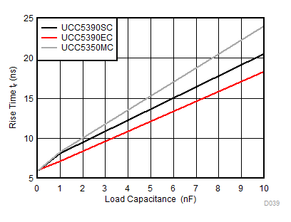
UCC5310 UCC5320 UCC5350 UCC5390 Rise Time vs Load Capacitance
fSW = 1 kHz RGH = 0 Ω RGL = 0 Ω
Figure 6-37 Rise Time vs Load Capacitance
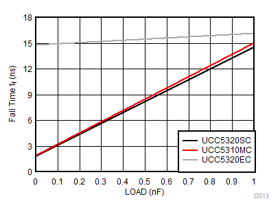
UCC5310 UCC5320 UCC5350 UCC5390 Fall Time vs Load Capacitance
fSW = 1 kHzRGH = 0 ΩRGL = 0 Ω
Figure 6-39 Fall Time vs Load Capacitance
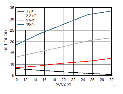
UCC5310 UCC5320 UCC5350 UCC5390 UCC5350SBD Fall Time vs CL and VCC2
Figure 6-41 UCC5350SBD Fall Time vs CL and VCC2
UCC5310 UCC5320 UCC5350 UCC5390 Output-High Drive Current vs Output Voltage
CLOAD = 150 nF
Figure 6-6 Output-High Drive Current vs Output Voltage
UCC5310 UCC5320 UCC5350 UCC5390 Output-Low Drive Current vs Output Voltage
CLOAD = 150 nF
Figure 6-8 Output-Low Drive Current vs Output Voltage
UCC5310 UCC5320 UCC5350 UCC5390 ICC1 Supply Current vs Temperature
IN+ = LIN– = H
Figure 6-10 ICC1 Supply Current vs Temperature
UCC5310 UCC5320 UCC5350 UCC5390 ICC1 Supply Current vs Temperature
IN+ = HIN– = L
Figure 6-12 ICC1 Supply Current vs Temperature
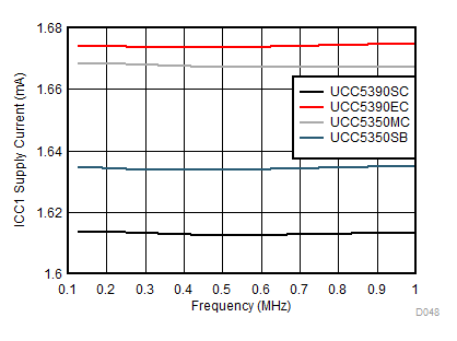
UCC5310 UCC5320 UCC5350 UCC5390 ICC1 Supply Current vs Input Frequency
Duty Cycle = 50%T = 25°C
Figure 6-14 ICC1 Supply Current vs Input Frequency
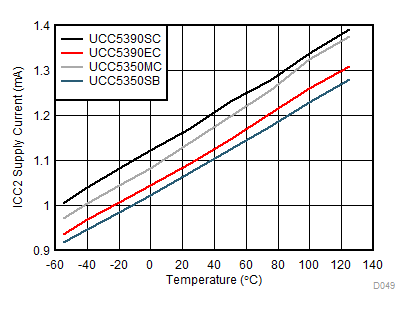
UCC5310 UCC5320 UCC5350 UCC5390 ICC2 Supply Current vs Temperature
IN+ = LIN– = H
Figure 6-16 ICC2 Supply Current vs Temperature
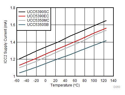
UCC5310 UCC5320 UCC5350 UCC5390 ICC2 Supply Current vs Temperature
IN+ = H IN– = L
Figure 6-18 ICC2 Supply Current vs Temperature
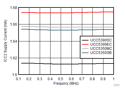
UCC5310 UCC5320 UCC5350 UCC5390 ICC2 Supply Current vs Input Frequency
Duty Cycle = 50%T = 25°C
Figure 6-20 ICC2 Supply Current vs Input Frequency
UCC5310 UCC5320 UCC5350 UCC5390 ICC2 Supply Current vs Load Capacitance
fSW = 1 kHz
Figure 6-22 ICC2 Supply Current vs Load Capacitance
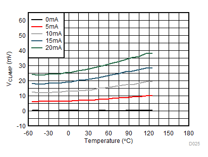
UCC5310 UCC5320 UCC5350 UCC5390 UCC5310M VClamp vs Temperature
IClamp = 0mA~20mA
Figure 6-24 UCC5310M VClamp vs Temperature
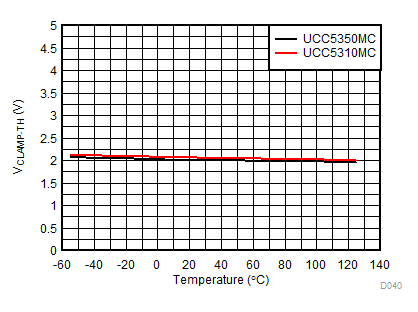
UCC5310 UCC5320 UCC5350 UCC5390 VClamp-TH vs Temperature
Figure 6-26 VClamp-TH vs Temperature
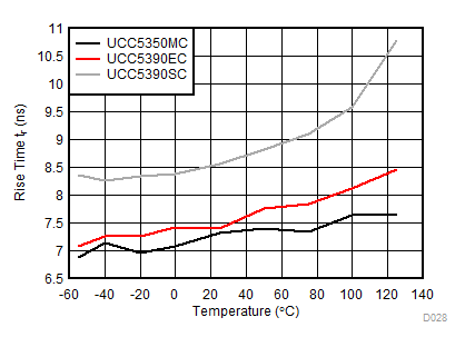
UCC5310 UCC5320 UCC5350 UCC5390 Rise Time vs Temperature
Figure 6-28 Rise Time vs Temperature
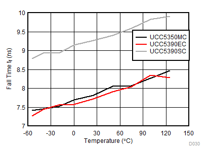
UCC5310 UCC5320 UCC5350 UCC5390 Fall Time vs Temperature
Figure 6-30 Fall Time vs Temperature
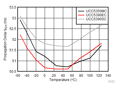
UCC5310 UCC5320 UCC5350 UCC5390 Propagation Delay tPLH vs Temperature
Figure 6-32 Propagation Delay tPLH vs Temperature
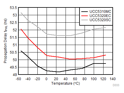
UCC5310 UCC5320 UCC5350 UCC5390 Propagation Delay tPHL vs Temperature
Figure 6-34 Propagation Delay tPHL vs Temperature
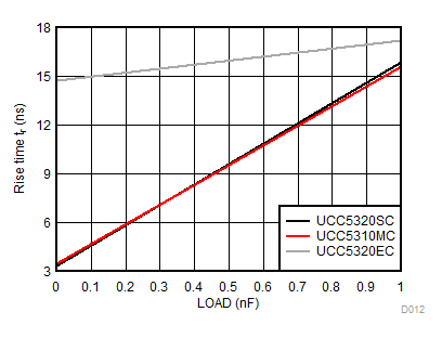
UCC5310 UCC5320 UCC5350 UCC5390 Rise Time vs Load Capacitance
fSW = 1 kHzRGH = 0 ΩRGL = 0 Ω
Figure 6-36 Rise Time vs Load Capacitance
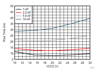
UCC5310 UCC5320 UCC5350 UCC5390 UCC5350SBD Rise Time vs CL and VCC2
Figure 6-38 UCC5350SBD Rise Time vs CL and VCC2
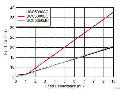
UCC5310 UCC5320 UCC5350 UCC5390 Fall Time vs Load Capacitance
fSW = 1 kHz RGH = 0 Ω RGL = 0 Ω
Figure 6-40 Fall Time vs Load Capacitance