SLLSER8J June 2017 – August 2024
PRODUCTION DATA
- 1
- 1 Features
- 2 Applications
- 3 Description
- 4 Device Comparison Table
- 5 Pin Configuration and Function
-
6 Specifications
- 6.1 Absolute Maximum Ratings
- 6.2 ESD Ratings
- 6.3 Recommended Operating Conditions
- 6.4 Thermal Information
- 6.5 Power Ratings
- 6.6 Insulation Specifications for D Package
- 6.7 Insulation Specifications for DWV Package
- 6.8 Safety-Related Certifications For D Package
- 6.9 Safety-Related Certifications For DWV Package
- 6.10 Safety Limiting Values
- 6.11 Electrical Characteristics
- 6.12 Switching Characteristics
- 6.13 Insulation Characteristics Curves
- 6.14 Typical Characteristics
- 7 Parameter Measurement Information
- 8 Detailed Description
- 9 Application and Implementation
- 10Power Supply Recommendations
- 11Layout
- 12Device and Documentation Support
- 13Revision History
- 14Mechanical, Packaging, and Orderable Information
9.2.3.3 Application Circuits with Output Stage Negative Bias
When parasitic inductances are introduced by nonideal PCB layout and long package leads (such as TO-220 and TO-247 type packages), ringing in the gate-source drive voltage of the power transistor could occur during high di/dt and dv/dt switching. If the ringing is over the threshold voltage, unintended turn-on and shoot-through could occur. Applying a negative bias on the gate drive is a popular way to keep such ringing below the threshold. A few examples of implementing negative gate-drive bias follow.
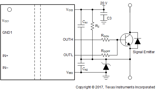
Figure 9-4 shows the first example with negative bias turn-off on the output using a Zener diode on the isolated power-supply output stage. The negative bias is set by the Zener diode voltage. If the isolated power supply is equal to 20 V, the turn-off voltage is –5.1 V and the turn-on voltage is 20 V – 5.1 V ≈ 15 V.
 Figure 9-4 Negative Bias With Zener Diode
on Iso-Bias Power-Supply Output
Figure 9-4 Negative Bias With Zener Diode
on Iso-Bias Power-Supply OutputFigure 9-5 shows another example which uses two supplies (or single-input, double-output power supply). The power supply across VCC2 and GND2 determines the positive drive output voltage and the power supply across VEE2 and GND2 determines the negative turn-off voltage. This solution requires more power supplies than the first example, however, it provides more flexibility when setting the positive and negative rail voltages.
 Figure 9-5 Negative Bias With Two
Iso-Bias Power Supplies (UCC5320E and
UCC5390E)