SLLSEY7F June 2017 – April 2020
PRODUCTION DATA.
- 1 Features
- 2 Applications
- 3 Description
- 4 Revision History
- 5 Pin Configuration and Functions
-
6 Specifications
- 6.1 Absolute Maximum Ratings
- 6.2 ESD Ratings
- 6.3 Recommended Operating Conditions
- 6.4 Thermal Information
- 6.5 Power Ratings
- 6.6 Insulation Specifications
- 6.7 Safety-Related Certifications
- 6.8 Safety Limiting Values
- 6.9 Electrical Characteristics—DC Specification
- 6.10 Switching Characteristics—AC Specification
- 6.11 Insulation Characteristics Curves
- 6.12 Typical Characteristics
- 7 Parameter Measurement Information
- 8 Detailed Description
- 9 Application and Implementation
- 10Power Supply Recommendations
- 11Layout
- 12Device and Documentation Support
- 13Mechanical, Packaging, and Orderable Information
9.2.1.2.2 Thermal Considerations
Thermal considerations constrain operation at different input current and voltage levels. The power dissipated inside the ISO121x devices is determined by the voltage at the SENSE pin (VSENSE) and the current drawn by the device (I(INx+SENSEx)). The internal power dissipated, when taken with the junction-to-air thermal resistance defined in the Thermal Information table can be used to determine the junction temperature for a given ambient temperature. The junction temperature must not exceed 150°C.
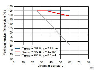
Figure 19 shows the maximum allowed ambient temperature for the ISO1211 device for different current limit and input voltage conditions. The ISO1211 device can be used with a VSENSE voltage up to 60 V and an ambient temperature of up to 125°C for an RSENSE value of 562 Ω, which corresponds to a typical current limit of 2.25 mA. At higher levels of current limit, either the ambient temperature or the maximum value of the VSENSE voltage must be derated. In any design, the voltage drop across the external series resistor, RTHR, reduces the maximum voltage received by the SENSE pin and helps extend the allowable module input voltage and ambient temperature range.

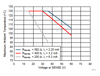
Figure 20 shows the maximum allowed ambient temperature for the ISO1212 device for different current limit and input voltage conditions. The ISO1212 device can be used with a VSENSE voltage up to 36 V and an ambient temperature of up to 125°C for an RSENSE value of 562 Ω, which corresponds to a typical current limit of 2.25 mA. At higher current limit levels, either the ambient temperature or the maximum value of the VSENSE voltage must be derated. Operation of the ISO1212 device with an RSENSE value of 200 Ω and with both channels active is not recommended beyond a VSENSE voltage of 36 V. In any design, the voltage drop across the series resistor, RTHR, reduces the maximum voltage received by the SENSE pin and helps extend the allowable module input voltage and ambient temperature range.
