SLLSF86C May 2018 – March 2022
PRODUCTION DATA
- 1 Features
- 2 Applications
- 3 Description
- 4 Revision History
- 5 Description Continued
- 6 Device Comparison Table
- 7 Pin Configuration and Functions
-
8 Specifications
- 8.1 Absolute Maximum Ratings
- 8.2 Recommended Operating Conditions
- 8.3 Thermal Information
- 8.4 Power Ratings
- 8.5 Insulation Specifications
- 8.6 Safety-Related Certifications
- 8.7 Safety Limiting Values
- 8.8 Electrical Characteristics
- 8.9 Supply Current Characteristics at VISOOUT = 3.3 V
- 8.10 Supply Current Characteristics at VISOOUT = 5 V
- 8.11 Switching Characteristics at VISOOUT = 3.3 V
- 8.12 Switching Characteristics at VISOOUT = 5 V
- 8.13 Insulation Characteristics Curves
- 8.14 Typical Characteristics
- 9 Parameter Measurement Information
- 10Detailed Description
- 11Application and Implementation
- 12Power Supply Recommendations
- 13Layout
- 14Device and Documentation Support
- 15Mechanical, Packaging, and Orderable Information
7 Pin Configuration and Functions
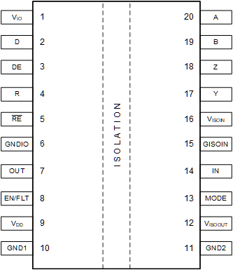
 Figure 7-1 ISOW14x220-pin DFMTop View
Table 7-1 Pin Functions
| PIN | I/O | DESCRIPTION | |
|---|---|---|---|
| NAME | NO. | ||
| VIO | 1 | -- | Side 1 logic supply |
| D | 2 | I | Data input |
| DE | 3 | I | Driver enable. If pin is floating, driver is disabled (internal pull-down resistor) |
| R | 4 | O | Received data output |
| RE | 5 | I | Receiver enable. If pin is floating, receiver buffer is disabled (internal pull-up resistor) |
| GNDIO | 6 | -- | Ground connections for VIO . GNDIO and GND1 need be shorted directly on PCB. |
| OUT | 7 | O | General purpose logic output |
| EN/FLT | 8 | I/O |
Multi-function power converter enable input pin or fault output pin. Can only be used as either an input pin or an output pin.
|
| VDD | 9 | -- | Side 1 DC-DC converter power supply |
| GND1 | 10 | -- | Ground connection for VIO. GNDIO and GND1 need be shorted directly on PCB. |
| GND2 | 11 | -- | Ground connection for VISOOUT. GND2 and GISOIN need be shorted direclty on PCB, or connected through a ferrite bead. |
| VISOOUT | 12 | -- | Isolated power converter output voltage. VISOOUT and VISOIN need be shorted directly on PCB, or connected through a ferrite bead. |
| MODE | 13 | I | Mode select. For RS-485 transceiver to operate at 3.3V supply, connect MODE to GND2. For RS-485 transceiver to operate in 5V supply PROFIBUS mode, connect MODE to VISOOUT (internal pull-down resistor) |
| IN | 14 | I | General purpose logic input |
| GISOIN | 15 | -- | Ground connections for VISOIN. GND2 and GISOIN need be shorted direclty on PCB, or connected through a ferrite bead. |
| VISOIN | 16 | -- | Side 2 supply voltage for RS485. VISOOUT and VISOIN need be shorted directly on PCB, or connected through a ferrite bead. |
| Y | 17 | O | RS-485 driver non-inverting output |
| Z | 18 | O | RS-485 driver inverting output |
| B | 19 | I | RS-485 receiver inverting input |
| A | 20 | I | RS-485 receiver non-inverting input |