SLLSF86C May 2018 – March 2022
PRODUCTION DATA
- 1 Features
- 2 Applications
- 3 Description
- 4 Revision History
- 5 Description Continued
- 6 Device Comparison Table
- 7 Pin Configuration and Functions
-
8 Specifications
- 8.1 Absolute Maximum Ratings
- 8.2 Recommended Operating Conditions
- 8.3 Thermal Information
- 8.4 Power Ratings
- 8.5 Insulation Specifications
- 8.6 Safety-Related Certifications
- 8.7 Safety Limiting Values
- 8.8 Electrical Characteristics
- 8.9 Supply Current Characteristics at VISOOUT = 3.3 V
- 8.10 Supply Current Characteristics at VISOOUT = 5 V
- 8.11 Switching Characteristics at VISOOUT = 3.3 V
- 8.12 Switching Characteristics at VISOOUT = 5 V
- 8.13 Insulation Characteristics Curves
- 8.14 Typical Characteristics
- 9 Parameter Measurement Information
- 10Detailed Description
- 11Application and Implementation
- 12Power Supply Recommendations
- 13Layout
- 14Device and Documentation Support
- 15Mechanical, Packaging, and Orderable Information
11.1 Application Information
The ISOW14x2 devices are designed for bidirectional data transfer on multipoint RS-485 networks. An RS-485 bus has multiple transceivers that connect in parallel to a bus cable. Both cable ends are terminated with a termination resistor, RT, to remove line reflections. The value of RT matches the characteristic impedance, Z0, of the cable. This method, known as parallel termination, lets higher data rates be used over a longer cable length.
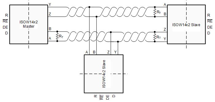
Full-duplex implementation shown in Figure 9-1 requires two signal pairs (four wires). Full-duplex implementation lets each node to transmit data on one pair while simultaneously receiving data on the other pair.
 Figure 11-1 Typical RS-485 network with Full-duplex Isolated transceivers
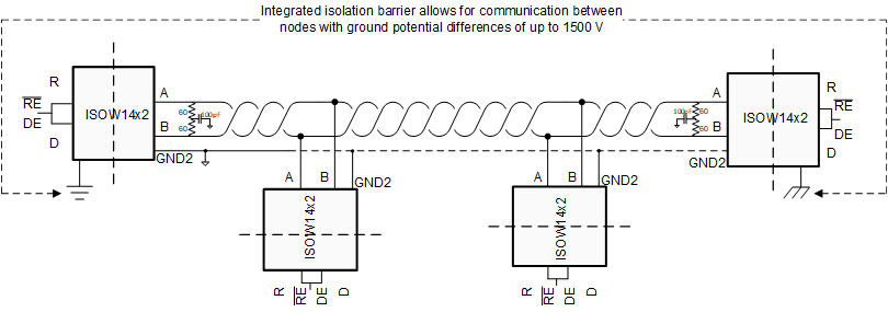
Figure 9-2 below, shows ISOW14x2 devices used in half duplex configuration. Driver outputs Y and Z are shorted to A and B respectively. This reduces overall cabling requirements. Also DE/RE are shorted to each other, and at a time, any node acts as either a driver or a receiver. Split termination is also shown in this configuration which helps to boost network immunity in noisy environments by providing common-mode noise filtering and also reduces radiated emissions by providing low impedance path to earth to the bus common mode excursions.
 Figure 11-2 Typical RS-485 Network With Half-Duplex Isolated Transceivers