SLLSF86C May 2018 – March 2022
PRODUCTION DATA
- 1 Features
- 2 Applications
- 3 Description
- 4 Revision History
- 5 Description Continued
- 6 Device Comparison Table
- 7 Pin Configuration and Functions
-
8 Specifications
- 8.1 Absolute Maximum Ratings
- 8.2 Recommended Operating Conditions
- 8.3 Thermal Information
- 8.4 Power Ratings
- 8.5 Insulation Specifications
- 8.6 Safety-Related Certifications
- 8.7 Safety Limiting Values
- 8.8 Electrical Characteristics
- 8.9 Supply Current Characteristics at VISOOUT = 3.3 V
- 8.10 Supply Current Characteristics at VISOOUT = 5 V
- 8.11 Switching Characteristics at VISOOUT = 3.3 V
- 8.12 Switching Characteristics at VISOOUT = 5 V
- 8.13 Insulation Characteristics Curves
- 8.14 Typical Characteristics
- 9 Parameter Measurement Information
- 10Detailed Description
- 11Application and Implementation
- 12Power Supply Recommendations
- 13Layout
- 14Device and Documentation Support
- 15Mechanical, Packaging, and Orderable Information
3 Description
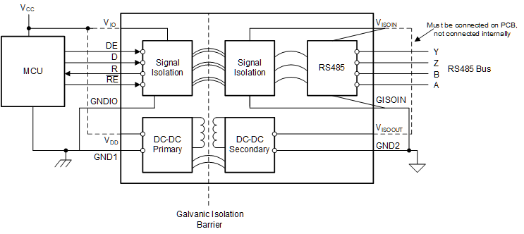
The ISOW14x2 devices are galvanically-isolated RS-485/RS-422 transceivers with a built-in isolated DC-DC converter, that eliminates the need for a separate isolated power supply in space constrained isolated designs. The low-emissions, isolated DC-DC converter meets CISPR 32 radiated emissions Class B standard with just two ferrite beads on a simple two-layer PCB. Additional 20 mA output current can be used to power other circuits on the board. An integrated 2 Mbps GPIO channel helps remove any additional digital isolator or optocoupler for diagnotstics, LED indication or supply monitoring.
Device
Information
| FEATURE | ISOW1412 ISOW1432 |
ISOW1412B ISOW1432B |
|---|---|---|
| Protection Level | Reinforced | Basic |
| Surge Test Voltage | 10 kVPK | 7.8 kVPK |
| Isolation Rating | 5000 VRMS | 5000 VRMS |
| Working Voltage | 1000 VRMS/1500 VPK | 1000 VRMS/1500 VPK |
| Package(1) | DFM (20) | DFM (20) |
| Body Size | 12.83 mm x 7.5 mm | 12.83 mm x 7.5 mm |
(1) For all available packages, see the
orderable addendum at the end of the data sheet.
 Simplified Schematic