SLLU327 May 2020 TUSB217A
6 TUSB217AEVM-BC Schematics
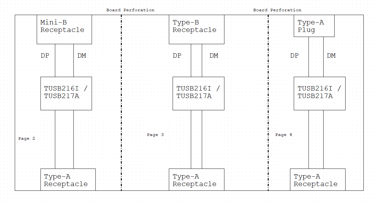
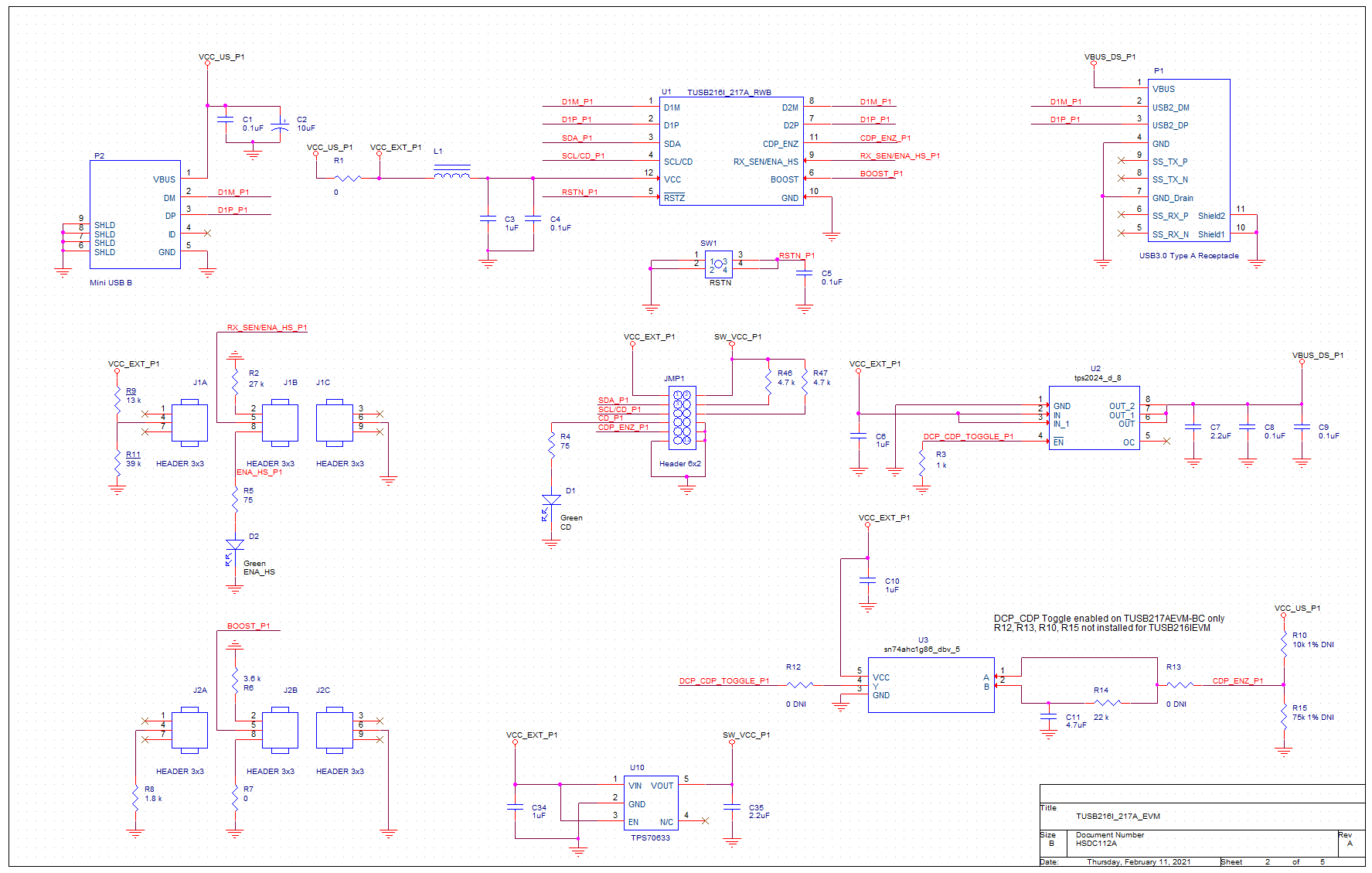
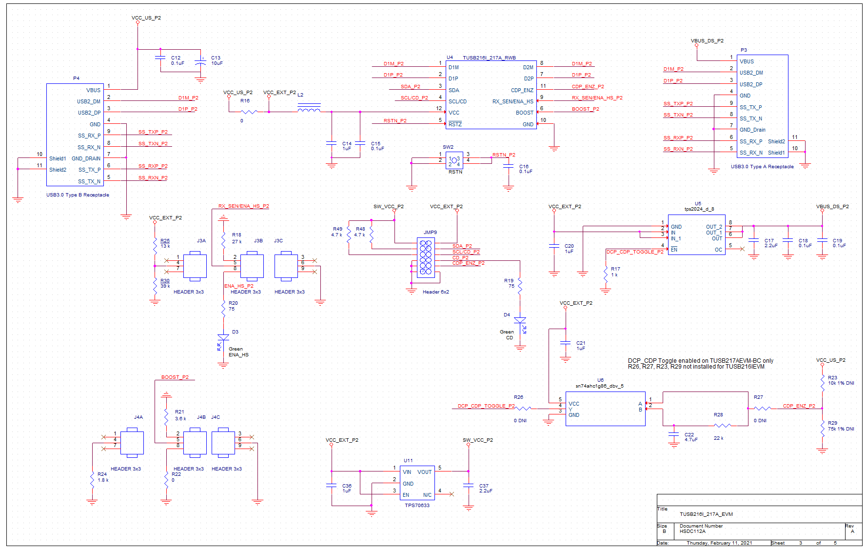
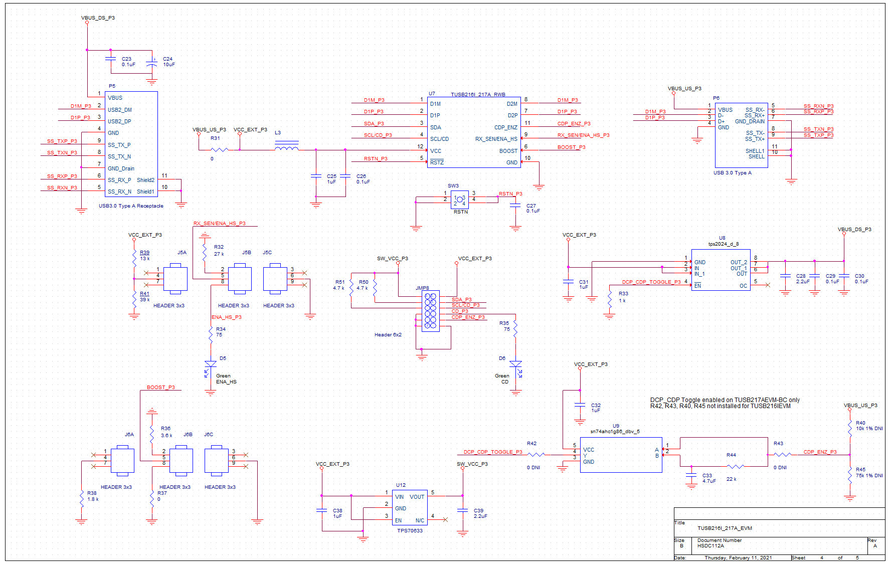
Figure 6-1 through Figure 6-4 show the EVM schematics.
 Figure 6-1 TUSB217AEVM-BC Block Diagram
 Figure 6-2 TUSB217AEVM-BC Mini-B Receptacle Section
 Figure 6-3 TUSB217AEVM-BC Type-B Receptacle Section
 Figure 6-4 TUSB217AEVM-BC Type-A Plug Section