SLOS438F December 2004 – March 2017 TPA2012D2
PRODUCTION DATA.
- 1 Features
- 2 Applications
- 3 Description
- 4 Revision History
- 5 Device Comparison Table
- 6 Pin Configuration and Functions
- 7 Specifications
- 8 Parameter Measurement Information
- 9 Detailed Description
- 10Application and Implementation
- 11Power Supply Recommendations
- 12Layout
- 13Device and Documentation Support
- 14Mechanical, Packaging, and Orderable Information
12 Layout
12.1 Layout Guidelines
12.1.1 Pad Side
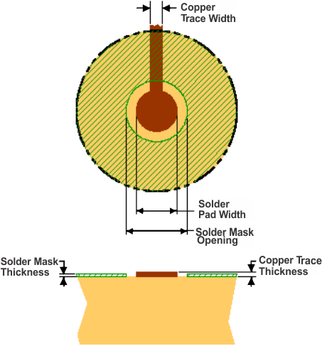
In making the pad size for the DSBGA balls, TI recommends that the layout use non-solder mask defined (NSMD) land. With this method, the solder mask opening is made larger than the desired land area, and the opening size is defined by the copper pad width. Figure 39 and Table 5 shows the appropriate diameters for a DSBGA layout. The TPA2012D2 evaluation module (EVM) layout is shown in the next section as a layout example.
Table 5. Land Pattern Dimensions(1)(3)(2)(4)
| SOLDER PAD DEFINITIONS |
COPPER PAD |
SOLDER MASK(5)
OPENING |
COPPER THICKNESS |
STENCIL(6)(7)
OPENING |
STENCIL THICKNESS |
|---|---|---|---|---|---|
| Nonsolder mask defined (NSMD) | 275 µm (+0.0, –25 µm) |
375 µm (+0.0, –25 µm) | 1 oz max (32 µm) | 275 µm × 275 µm (square) (rounded corners) |
125 µm |
 Figure 39. Land Pattern Dimensions
12.1.2 Component Location
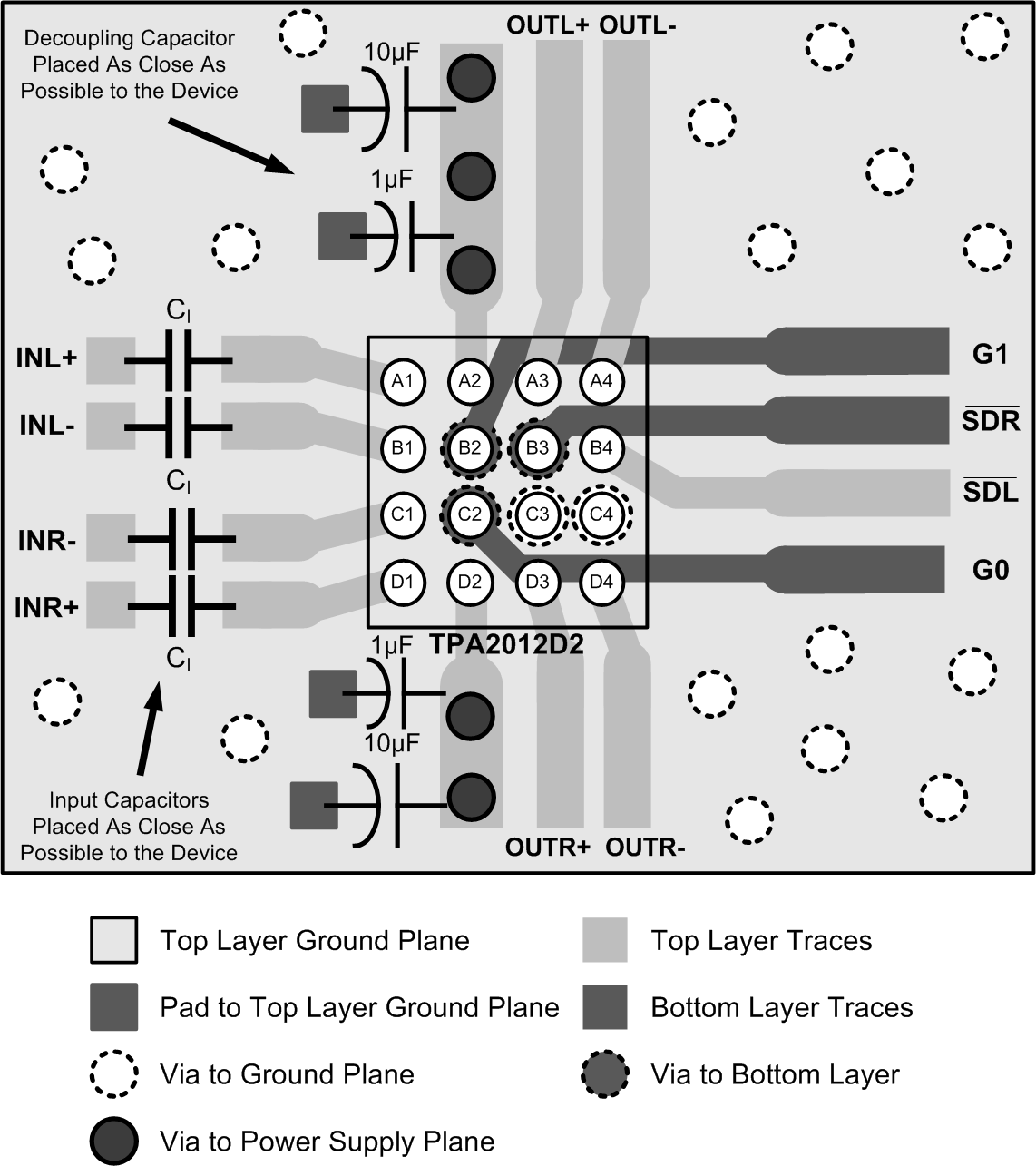
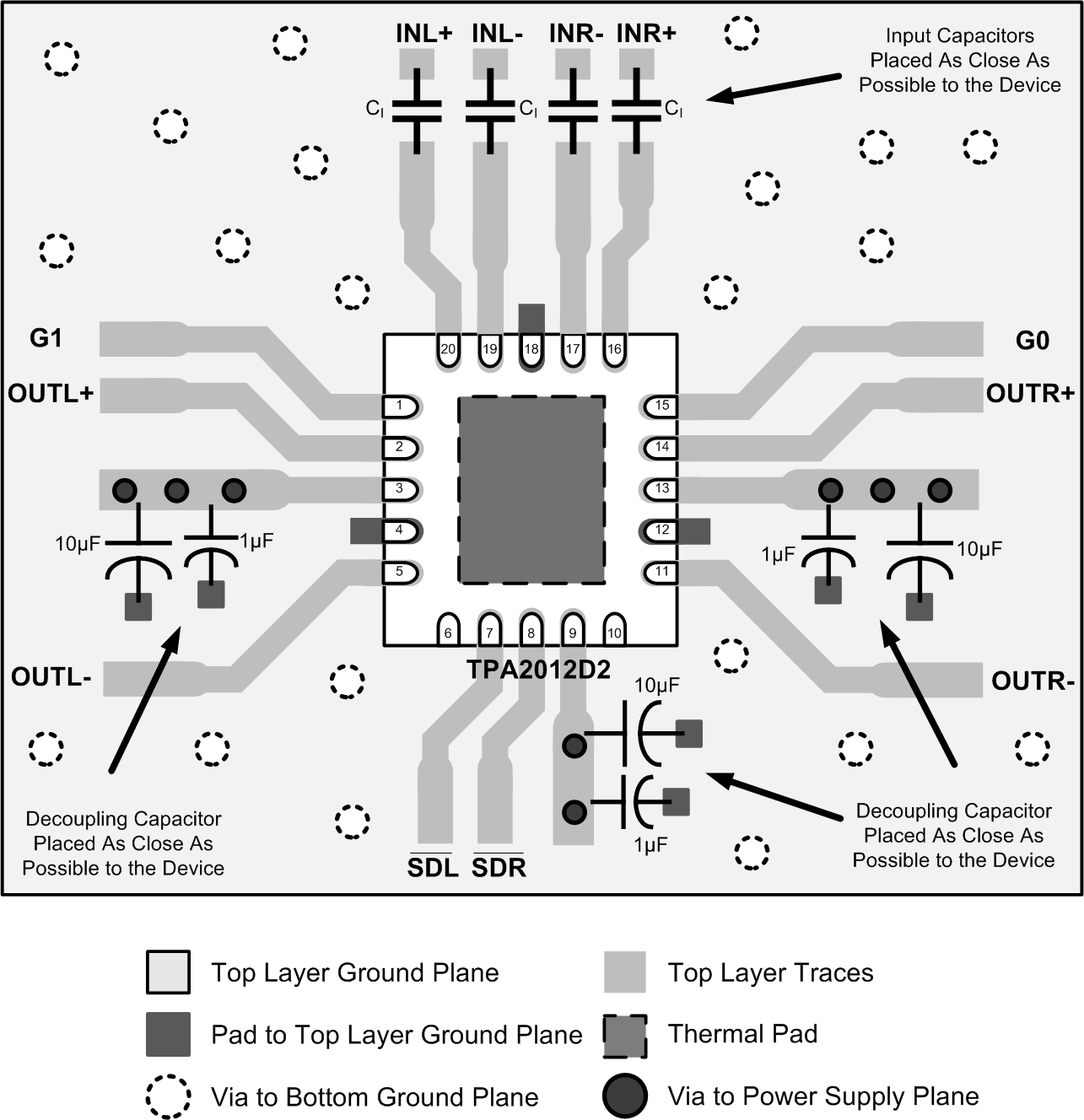
Place all the external components very close to the TPA2012D2. Placing the decoupling capacitor, CS, close to the TPA2012D2 is important for the efficiency of the Class-D amplifier. Any resistance or inductance in the trace between the device and the capacitor can cause a loss in efficiency.
12.1.3 Trace Width
Recommended trace width at the solder balls is 75 µm to 100 µm to prevent solder wicking onto wider PCB traces.
For high current pins (PVDD, PGND, and audio output pins) of the TPA2012D2, use 100-µm trace widths at the solder balls and at least 500-µm PCB traces to ensure proper performance and output power for the device.
For the remaining signals of the TPA2012D2, use 75-µm to 100-µm trace widths at the solder balls. The audio input pins (INR± and INL±) must run side-by-side to maximize common-mode noise cancellation.
12.2 Layout Examples
 Figure 40. TPA2012D2 DSBGA Layout Example
 Figure 41. TPA2012D2 WQFN Layout Example
12.3 Efficiency and Thermal Considerations
The maximum ambient temperature depends on the heat-sinking ability of the PCB system. The derating factor for the packages are shown in the dissipation rating table. Converting this to θJA for the WQFN package with Equation 3.

Given θJA of 24°C/W, the maximum allowable junction temperature of 150°C, and the maximum internal dissipation of 1.5 W (0.75 W per channel) for 2.1 W per channel, 4-Ω load, 5-V supply, from Figure 25, the maximum ambient temperature can be calculated with Equation 4.

Equation 4 shows that the calculated maximum ambient temperature is 114°C at maximum power dissipation with a 5-V supply and a 4-Ω load. The TPA2012D2 is designed with thermal protection that turns the device off when the junction temperature surpasses 150°C to prevent damage to the IC. Also, using speakers more resistive than 4-Ω dramatically increases the thermal performance by reducing the output current and increasing the efficiency of the amplifier.