SLOS528F July 2009 – April 2017 TPA3110D2
PRODUCTION DATA.
- 1 Features
- 2 Applications
- 3 Description
- 4 Revision History
- 5 Device Comparison Table
- 6 Pin Configuration and F unctions
- 7 Specifications
- 8 Parameter Measurement Information
-
9 Detailed Description
- 9.1 Overview
- 9.2 Functional Block Diagram
- 9.3 Feature Description
- 9.4 Device Functional Modes
- 10Application and Implementation
- 11Power Supply Recommendations
- 12Layout
- 13Device and Documentation Support
- 14Mechanical, Packaging, and Orderable Information
10 Application and Implementation
NOTE
Information in the following applications sections is not part of the TI component specification, and TI does not warrant its accuracy or completeness. TI’s customers are responsible for determining suitability of components for their purposes. Customers should validate and test their design implementation to confirm system functionality.
10.1 Application Information
This section describes a stereo BTL application and a mono PBTL application. In the stereo application the Power Limiter is implemented, however in the mono application this limiter is not used.
10.2 Typical Applications
10.2.1 Stereo Class-D Amplifier With BTL Output and Single-Ended Inputs With Power Limiting
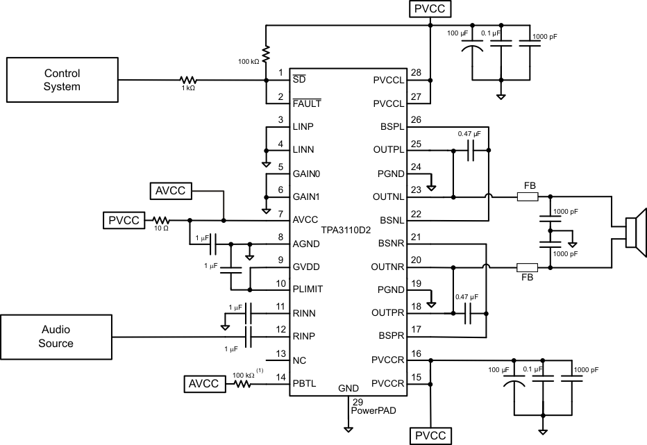
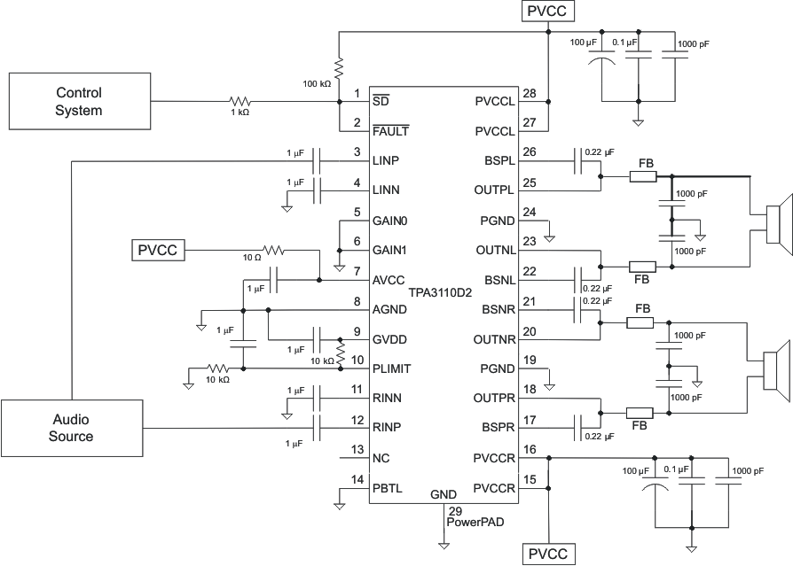 Figure 42. Typical Application Schematic With BTL Output and Single-Ended Inputs With Power Limiting
10.2.1.1 Design Requirements
For this design example, use the parameters listed in Table 5.
Table 5. Design Parameters
| DESIGN PARAMETER | EXAMPLE VALUE |
|---|---|
| Power supply | 8 V to 26 V |
| Shutdown, gain, and PBTL controls | High > 2 V |
| Low < 0.8 V | |
| Speaker impedance BTL | 4 to 8 Ω |
| Speaker impedance PBTL | 2 to 8 Ω |
10.2.1.2 Detailed Design Procedure
10.2.1.2.1 Input Resistance
Changing the gain setting can vary the input resistance of the amplifier from its smallest value, 9 kΩ ±20%, to the largest value, 60 kΩ ±20%. As a result, if a single capacitor is used in the input high-pass filter, the –3 dB or cutoff frequency may change when changing gain steps.
 Figure 43. Input Impedance of the TPA3110D2
The –3-dB frequency can be calculated using Equation 2. Use the ZI values given in Table 2.

10.2.1.2.2 Input Capacitor, CI
In the typical application, an input capacitor (CI) is required to allow the amplifier to bias the input signal to the proper dc level for optimum operation. In this case, CI and the input impedance of the amplifier (ZI) form a high-pass filter with the corner frequency determined in Equation 3.
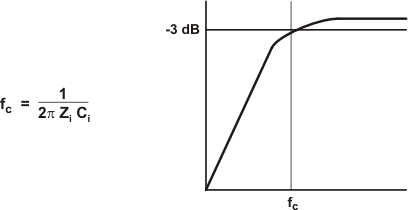
The value of CI is important, as it directly affects the bass (low-frequency) performance of the circuit. Consider the example where ZI is 60 kΩ and the specification calls for a flat bass response down to 20 Hz. Equation 3 is reconfigured as Equation 4.

In this example, CI is 0.13 µF; so, one would likely choose a value of 0.15 μF as this value is commonly used. If the gain is known and is constant, use ZI from Table 2 to calculate CI. A further consideration for this capacitor is the leakage path from the input source through the input network (CI) and the feedback network to the load. This leakage current creates a dc offset voltage at the input to the amplifier that reduces useful headroom, especially in high gain applications. For this reason, a low-leakage tantalum or ceramic capacitor is the best choice. When polarized capacitors are used, the positive side of the capacitor should face the amplifier input in most applications as the dc level there is held at 3 V, which is likely higher than the source dc level. Note that it is important to confirm the capacitor polarity in the application. Additionally, lead-free solder can create dc offset voltages and it is important to ensure that boards are cleaned properly.
10.2.1.2.3 BSN and BSP Capacitors
The full H-bridge output stages use only NMOS transistors. Therefore, they require bootstrap capacitors for the high side of each output to turn on correctly. A 0.22 μF ceramic capacitor, rated for at least 25 V, must be connected from each output to its corresponding bootstrap input. Specifically, one 0.22 μF capacitor must be connected from OUTPx to BSPx, and one 0.22 μF capacitor must be connected from OUTNx to BSNx. (See the application circuit diagram in Figure 42.)
The bootstrap capacitors connected between the BSxx pins and corresponding output function as a floating power supply for the high-side N-channel power MOSFET gate drive circuitry. During each high-side switching cycle, the bootstrap capacitors hold the gate-to-source voltage high enough to keep the high-side MOSFETs turned on.
10.2.1.2.4 Using Low-ESR Capacitors
Low-ESR capacitors are recommended throughout this application section. A real (as opposed to ideal) capacitor can be modeled simply as a resistor in series with an ideal capacitor. The voltage drop across this resistor minimizes the beneficial effects of the capacitor in the circuit. The lower the equivalent value of this resistance, the more the real capacitor behaves like an ideal capacitor.
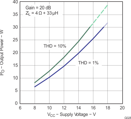
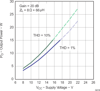
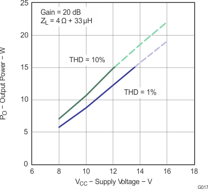
10.2.1.3 Application Curves
10.2.2 Stereo Class-D Amplifier With PBTL Output and Single-Ended Input
10.2.2.1 Design Requirements
Refer to Table 5 for the Stereo Class-D Amplifier With PBTL Output and Single-Ended Input Application Design Requirements.
10.2.2.2 Detailed Design Procedure
Refer to Detailed Design Procedure for the Stereo Class-D Amplifier With PBTL Output and Single-Ended Input Application Detailed Design Procedure.
10.2.2.3 Application Curve
