SLOS630C December 2010 – November 2014 TLV320AIC3256
PRODUCTION DATA.
- 1 Features
- 2 Applications
- 3 Description
- 4 Simplified Block Diagram
- 5 Revision History
- 6 Device Comparison Table
- 7 Pin Configuration and Functions
-
8 Specifications
- 8.1 Absolute Maximum Ratings
- 8.2 Handling Ratings
- 8.3 Recommended Operating Conditions
- 8.4 Thermal Information
- 8.5 Electrical Characteristics, ADC
- 8.6 Electrical Characteristics, Bypass Outputs
- 8.7 Electrical Characteristics, Microphone Interface
- 8.8 Electrical Characteristics, Audio DAC Outputs
- 8.9 Electrical Characteristics, Misc.
- 8.10 Electrical Characteristics, Logic Levels
- 8.11 I2S/LJF/RJF Timing in Master Mode (see )
- 8.12 I2S/LJF/RJF Timing in Slave Mode (see )
- 8.13 DSP Timing in Master Mode (see )
- 8.14 DSP Timing in Slave Mode (see )
- 8.15 Digital Microphone PDM Timing (see )
- 8.16 I2C Interface Timing
- 8.17 SPI Interface Timing
- 8.18 Typical Characteristics
- 9 Parameter Measurement Information
- 10Detailed Description
- 11Application and Implementation
- 12Power Supply Recommendations
- 13Layout
- 14Device and Documentation Support
- 15Mechanical, Packaging, and Orderable Information
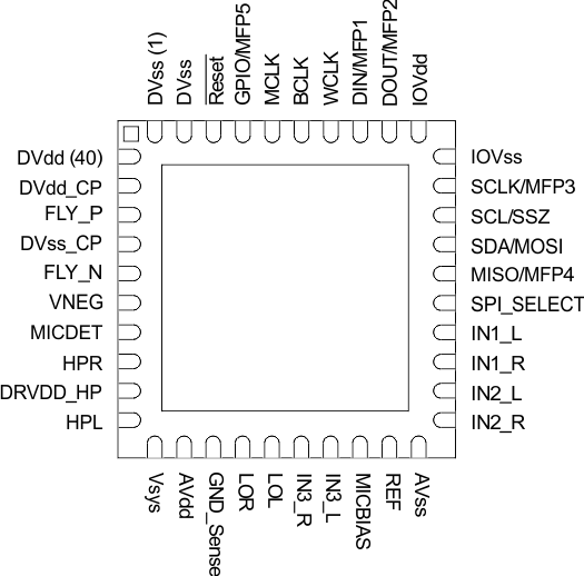
7 Pin Configuration and Functions
QFN
(RSB) Package
Bottom View

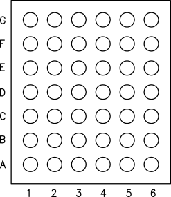
WCSP
(YZF) Package
Bottom View

Pin Functions
| PIN | WCSP (YZF) BALL NO. |
TYPE(1) | DESCRIPTION | ||
|---|---|---|---|---|---|
| NAME | QFN (RSB) NO. | ||||
| DVss | 1 | B2 | GND | Digital ground. Device substrate. | |
| DVss | 2 | A1 | GND | Digital ground | |
| RESET | 3 | C5 | DI | Hardware reset | |
| GPIO | 4 | B3 | DI/O | Primary function: | |
| General purpose digital IO | |||||
| MFP5 | Secondary function: | ||||
| CLKOUT output INT1 output INT2 output Audio serial data bus ADC word clock output Audio serial data bus (secondary) bit clock output Audio serial data bus (secondary) word clock output Digital microphone clock output |
|||||
| MCLK | 5 | A2 | DI | Master clock input | |
| BCLK | 6 | B4 | DI/O | Audio serial data bus (primary) bit clock | |
| WCLK | 7 | A3 | DI/O | Audio serial data bus (primary) word clock | |
| DIN | 8 | A5 | DI | Primary function: | |
| Audio serial data bus data input | |||||
| MFP1 | Secondary function: | ||||
| Digital Microphone Input General Purpose Clock Input General Purpose Input |
|||||
| DOUT | 9 | A4 | DO | Primary function: | |
| Audio serial data bus data output | |||||
| MFP2 | Secondary function: | ||||
| General purpose output Clock output INT1 output INT2 output Audio serial data bus (secondary) bit clock output Audio serial data bus (secondary) word clock output |
|||||
| IOVdd | 10 | A6 | PWR | Supply for IO buffers. 1.1V to 3.6V | |
| IOVss | 11 | B5 | GND | Ground for IO buffers. | |
| SCLK | 12 | C4 | DI | Primary function: (SPI_Select = 1) | |
| SPI serial clock | |||||
| MFP3 | Secondary function:: (SPI_Select = 0) | ||||
| Digital microphone input Audio serial data bus (secondary) bit clock input Audio serial data bus (secondary) DAC/common word clock input Audio serial data bus (secondary) ADC word clock input Audio serial data bus (secondary) data input General purpose input |
|||||
| SCL SS |
13 | B6 | DI | I2C interface serial clock (SPI_Select = 0) SPI interface mode chip-select signal (SPI_Select = 1) |
|
| SDA MOSI |
14 | C3 | DI/O | I2C interface mode serial data input (SPI_Select = 0) SPI interface mode serial data input (SPI_Select = 1) |
|
| MISO | 15 | D4 | DO | Primary function: (SPI_Select = 1) | |
| Serial data output | |||||
| MFP4 | Secondary function: (SPI_Select = 0) | ||||
| General purpose output CLKOUT output INT1 output INT2 output Audio serial data bus (primary) ADC word clock output Digital microphone clock output Audio serial data bus (secondary) data output Audio serial data bus (secondary) bit clock output Audio serial data bus (secondary) word clock output |
|||||
| SPI_SELECT | 16 | C6 | DI | Control mode select pin ( 1 = SPI, 0 = I2C ) | |
| IN1_L | 17 | D6 | AI | Multifunction analog input, Single-ended configuration: MIC 1 or Line 1 left Differential configuration: MIC or Line right, negative |
|
| IN1_R | 18 | E6 | AI | Multifunction analog input, Single-ended configuration: MIC 1 or Line 1 right Differential configuration: MIC or Line right, positive |
|
| IN2_L | 19 | F6 | AI | Multifunction analog input, Single-ended configuration: MIC 2 or Line 2 right Differential configuration: MIC or Line left, positive |
|
| IN2_R | 20 | G6 | AI | Multifunction analog input, Single-ended configuration: MIC 2 or Line 2 right Differential configuration: MIC or Line left, negative |
|
| AVss | 21 | E4, E5 | GND | Analog Ground | |
| REF | 22 | G5 | AO | Reference voltage output for filtering | |
| MICBIAS | 23 | G4 | AO | Microphone bias voltage output | |
| IN3_L | 24 | F5 | AI | Multifunction analog input, Single-ended configuration: MIC3 or Line 3 left, Differential configuration: MIC or Line left, positive, Differential configuration: MIC or Line right, negative |
|
| IN3_R | 25 | F4 | AI | Multifunction analog input, Single-ended configuration: MIC3 or Line 3 right, Differential configuration: MIC or Line left, negative, Differential configuration: MIC or Line right, positive |
|
| LOL | 26 | G3 | AO | Left line output | |
| LOR | 27 | F3 | AO | Right line output | |
| GND_SENSE | 28 | E3 | AI | External ground reference for headphone interface –0.5V to 0.5V | |
| AVdd | 29 | G2 | PWR | Analog voltage supply 1.5V–1.95V | |
| Vsys | 30 | G1 | PWR | Power supply 1.5V–5.5V, Vsys must always be greater than or equal to AVdd and DVdd (Vsys ≥ AVdd, DVdd) | |
| HPL | 31 | F1 | AO | Left headphone output | |
| DRVdd_HP | 32 | F2 | PWR | Power supply for headphone output stage Ground-centered circuit configuration, 1.5V to 1.95V Unipolar circuit configuration, 1.5V to 3.6V |
|
| HPR | 33 | E1 | AO | Right headphone output | |
| MICDET | 34 | E2 | AI | Microphone detection | |
| VNEG | 35 | D1 | PWR | Negative supply for headphones. –1.8V to 0V Input when charge pump is disabled, Filtering output when charge pump is enabled |
|
| FLY_N | 36 | D2 | PWR | Negative terminal for charge-pump flying capacitor | |
| DVss_CP | 37 | D3 | GND | Charge pump ground | |
| FLY_P | 38 | C2 | PWR | Positive terminal for charge pump flying capacitor | |
| DVdd_CP | 39 | C1 | PWR | Charge Pump supply; recommended to connect to DVdd | |
| DVdd | 40 | B1 | PWR | Digital voltage supply 1.26V – 1.95V | |
| Thermal Pad | Thermal Pad | N/A | N/A | Connect to PCB ground plane. Not internally connected. | |