SLPS223F May 2010 – October 2016 CSD86350Q5D
PRODUCTION DATA.
6 Application and Implementation
NOTE
Information in the following applications sections is not part of the TI component specification, and TI does not warrant its accuracy or completeness. TI’s customers are responsible for determining suitability of components for their purposes. Customers should validate and test their design implementation to confirm system functionality.
6.1 Application Information
6.1.1 Equivalent System Performance
Many of today’s high-performance computing systems require low-power consumption in an effort to reduce system operating temperatures and improve overall system efficiency. This has created a major emphasis on improving the conversion efficiency of today’s synchronous buck topology. In particular, there has been an emphasis in improving the performance of the critical power semiconductor in the power stage of this application (see Figure 28). As such, optimization of the power semiconductors in these applications, needs to go beyond simply reducing RDS(ON).
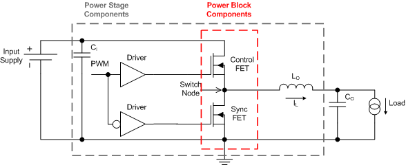 Figure 28. Equivalent System Schematic
The CSD86350Q5D is part of TI’s power block product family which is a highly optimized product for use in a synchronous buck topology requiring high-current, high-efficiency, and high-frequency. It incorporates TI’s latest generation silicon which has been optimized for switching performance, as well as minimizing losses associated with QGD, QGS, and QRR. Furthermore, TI’s patented packaging technology has minimized losses by nearly eliminating parasitic elements between the control FET and sync FET connections (see Figure 29). A key challenge solved by TI’s patented packaging technology is the system-level impact of Common Source Inductance (CSI). CSI greatly impedes the switching characteristics of any MOSFET which in turn increases switching losses and reduces system efficiency. As a result, the effects of CSI need to be considered during the MOSFET selection process. In addition, standard MOSFET switching loss equations used to predict system efficiency need to be modified in order to account for the effects of CSI. Further details behind the effects of CSI and modification of switching loss equations are outlined in Power Loss Calculation With Common Source Inductance Consideration for Synchronous Buck Converters (SLPA009).
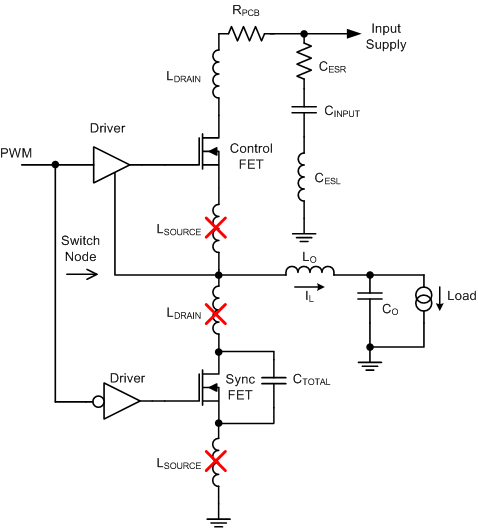 Figure 29. Elimination of Parasitic Inductances
The combination of TI’s latest generation silicon and optimized packaging technology has created a benchmarking solution that outperforms industry standard MOSFET chipsets of similar RDS(ON) and MOSFET chipsets with lower RDS(ON). Figure 30 and Figure 31 compare the efficiency and power loss performance of the CSD86350Q5D versus industry standard MOSFET chipsets commonly used in this type of application. This comparison purely focuses on the efficiency and generated loss of the power semiconductors only. The performance of CSD86350Q5D clearly highlights the importance of considering the effective AC on-impedance (ZDS(ON)) during the MOSFET selection process of any new design. Simply normalizing to traditional MOSFET RDS(ON) specifications is not an indicator of the actual in-circuit performance when using TI’s power block technology.

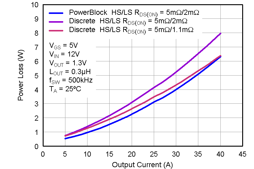
Table 1 below compares the traditional DC measured RDS(ON) of CSD86350Q5D versus its ZDS(ON). This comparison takes into account the improved efficiency associated with TI’s patented packaging technology. As such, when comparing TI’s power block products to individually packaged discrete MOSFETs or dual MOSFETs in a standard package, the in-circuit switching performance of the solution must be considered. In this example, individually packaged discrete MOSFETs or dual MOSFETs in a standard package would need to have DC measured RDS(ON) values that are equivalent to CSD86350Q5D’s ZDS(ON) value in order to have the same efficiency performance at full load. Mid to light-load efficiency will still be lower with individually packaged discrete MOSFETs or dual MOSFETs in a standard package.
Table 1. Comparison of RDS(ON) vs. ZDS(ON)
| PARAMETER | HS | LS | ||
|---|---|---|---|---|
| TYP | MAX | TYP | MAX | |
| Effective AC on-impedance (ZDS(ON)), VGS = 5 V | 5 | — | 1.1 | — |
| DC measured RDS(ON), VGS = 4.5 V | 5 | 6.6 | 2 | 2.7 |
The CSD86350Q5D NexFET™ power block is an optimized design for synchronous buck applications using 5-V gate drive. The control FET and sync FET silicon are parametrically tuned to yield the lowest power loss and highest system efficiency. As a result, a new rating method is needed which is tailored towards a more systems-centric environment. System-level performance curves such as power loss, Safe Operating Area (SOA), and normalized graphs allow engineers to predict the product performance in the actual application.
6.1.2 Power Loss Curves
MOSFET centric parameters such as RDS(ON) and Qgd are needed to estimate the loss generated by the devices. In an effort to simplify the design process for engineers, Texas Instruments has provided measured power loss performance curves. Figure 1 plots the power loss of the CSD86350Q5D as a function of load current. This curve is measured by configuring and running the CSD86350Q5D as it would be in the final application (see Figure 32).The measured power loss is the CSD86350Q5D loss and consists of both input conversion loss and gate drive loss. Equation 1 is used to generate the power loss curve.
The power loss curve in Figure 1 is measured at the maximum recommended junction temperatures of 125°C under isothermal test conditions.
6.1.3 Safe Operating Area (SOA) Curves
The SOA curves in the CSD86350Q5D data sheet provides guidance on the temperature boundaries within an operating system by incorporating the thermal resistance and system power loss. Figure 3 to Figure 5 outline the temperature and airflow conditions required for a given load current. The area under the curve dictates the safe operating area. All the curves are based on measurements made on a PCB design with dimensions of 4 in (W) × 3.5 in (L) × 0.062 in (T) and 6 copper layers of 1-oz copper thickness.
6.1.4 Normalized Curves
The normalized curves in the CSD86350Q5D data sheet provides guidance on the power loss and SOA adjustments based on their application specific needs. These curves show how the power loss and SOA boundaries will adjust for a given set of systems conditions. The primary Y-axis is the normalized change in power loss and the secondary Y-axis is the change in system temperature required in order to comply with the SOA curve. The change in power loss is a multiplier for the power loss curve and the change in temperature is subtracted from the SOA curve.
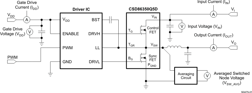 Figure 32. Typical Application
6.1.5 Calculating Power Loss and SOA
The user can estimate product loss and SOA boundaries by arithmetic means (see Design Example). Though the power loss and SOA curves in this data sheet are taken for a specific set of test conditions, the following procedure will outline the steps the user should take to predict product performance for any set of system conditions.
6.1.5.1 Design Example
Operating Conditions:
- Output Current = 25 A
- Input Voltage = 7 V
- Output Voltage = 1 V
- Switching Frequency = 800 kHz
- Inductor = 0.2 µH
6.1.5.2 Calculating Power Loss
- Power loss at 25 A = 3.5 W (Figure 1)
- Normalized power loss for input voltage ≈ 1.07 (Figure 7)
- Normalized power loss for output voltage ≈ 0.95 (Figure 8)
- Normalized power loss for switching frequency ≈ 1.11 (Figure 6)
- Normalized power loss for output inductor ≈ 1.07 (Figure 9)
- Final calculated power loss = 3.5 W × 1.07 × 0.95 × 1.11 × 1.07 ≈ 4.23 W
6.1.5.3 Calculating SOA Adjustments
In the design example above, the estimated power loss of the CSD86350Q5D would increase to 4.23 W. In addition, the maximum allowable board and/or ambient temperature would have to decrease by 5.1°C. Figure 33 graphically shows how the SOA curve would be adjusted accordingly.
- Start by drawing a horizontal line from the application current to the SOA curve.
- Draw a vertical line from the SOA curve intercept down to the board/ambient temperature.
- Adjust the SOA board/ambient temperature by subtracting the temperature adjustment value.
In the design example, the SOA temperature adjustment yields a reduction in allowable board/ambient temperature of 5.1°C. In the event the adjustment value is a negative number, subtracting the negative number would yield an increase in allowable board/ambient temperature.
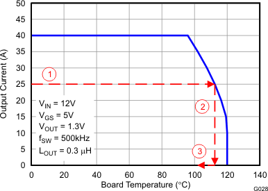 Figure 33. Power Block SOA