SLUA748A December   2015  – April 2016 BQ25120 , BQ51003 , TPS61046 , TPS61240 , TPS62743


  1.   Trademarks
  2.   Power Management Reference Design for a Wearable Device with Wireless Charging Using the bq51003 and bq25120
    1. 1 Wearable Power Design
      1. 1.1 Wireless Charging Input
      2. 1.2 Battery Charger, MCU, Radio, and Sensor Power
      3. 1.3 Second Buck Output for MCU, Radio or Sensor
    2. 2 PMOLED Display Power Design
    3. 3 Heart Rate Monitor or e-Ink Power Design
    4. 4 Layout Guidelines for Wearable Design
      1. 4.1 Wireless Receiver (bq51003)
      2. 4.2 Linear Charger (bq25120)
      3. 4.3 Buck Converter (TPS62743/6)
      4. 4.4 Boost Converters (TPS61046 and TPS61240)
      5. 4.5 General Considerations
    5. 5 References
  3. AExperimental Results
    1. A.1 Experimental Results
  4.   Revision History

Buck Converter (TPS62743/6)

  • The input capacitor must be placed close to the Vin pin of the IC.
  • The switching node should be as short as possible.
  • Connect the output cap with a trace –no via- away from the SW node and noisy signals.
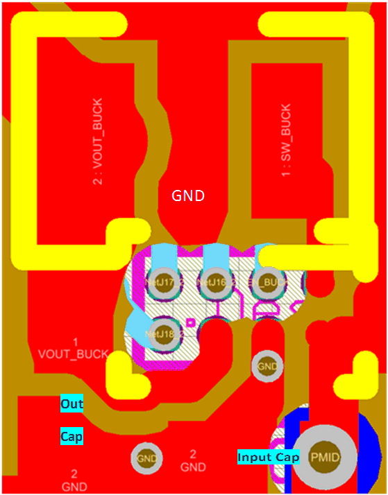
PCB_layout_TPS62743_slua748.gifFigure 9. TPS62743 Layout