SLUA748A December 2015 – April 2016 BQ25120 , BQ51003 , TPS61046 , TPS61240 , TPS62743
- Trademarks
- Power Management Reference Design for a Wearable Device with Wireless Charging Using the bq51003 and bq25120
- AExperimental Results
- Revision History
4.2 Linear Charger (bq25120)
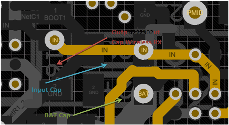
- Input capacitor (C21) must be placed close to the IC input pin. It is recommended to place the BAT capacitor close to the pin. Therefore, in this design the input trace coming from the output of the wireless receiver is connected through a via in an inner layer in order to reduce the size of the solution.
- The inductor should be placed close to the SW pin to reduce the size of the switching node.
- The output capacitors for the power rails (SYS, PMID, LS/LDO) need to be placed close to the pins.
 Figure 8. bq25120 Capacitors Placement