SLUA749A July 2015 – May 2016 BQ76920 , BQ76930 , BQ76940
4 Cell Balance
The bq769x0 devices have internal balance FETs controlled by the host through registers. When enabled, the internal FET will pull the pins associated with that cell together drawing current through the input resistors for that cell. For the bq76920 the input resistors can be sized to select the balance current within the capability of the part. For the bq76930 and bq76940, the input filter resistors must be large due to the device architecture, so internal balance current is limited in these family members.
The 250 ms measurement timeline is divided into 12.5 ms intervals. When balancing, the balance FET is enabled for 14 of the 20 intervals. The balance FET is turned off for one interval before measurement starts on the bottom cell of the group. The cells are then measured in sequence. The input filter must settle within the 12.5 ms or there will be voltage error in the cell measurement. Since the cells are measured in sequence, the bottom cells will show the largest influence. The more cells are balanced, the more time will be required for the filter to settle. For the bq76920, the Rc input resistors are adjusted for the balance current and are typically in the smaller values of the datasheet range, and the Cc filter capacitors can generally be large. For the bq76930 and bq76940 the input resistors are large and the Cc capacitors may be smaller for improved measurement.
Since the cell inputs pull together during balancing, care must be used to prevent damage to the inputs. If all cells in a group are enabled to balance at the same time, the inputs will pull together and some of the maximum limits will be exceeded, the part is likely to be damaged. Balancing every other cell in a group will double the voltage on the unbalanced cell and is typically OK, check the voltage limits for the cell voltages used in your design.
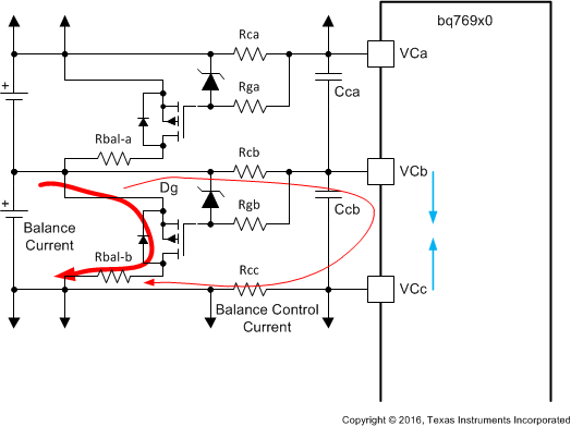
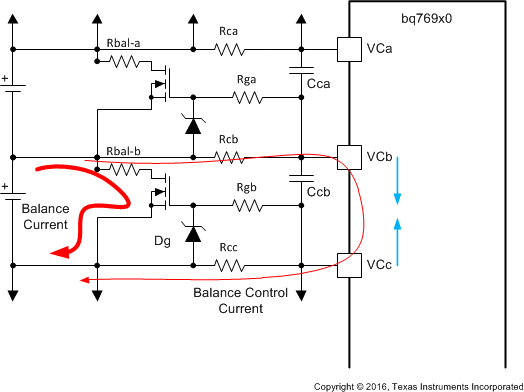
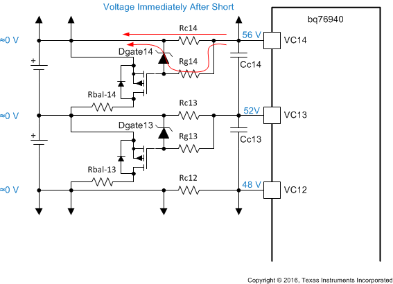
External cell balancing can be used with the bq769x0 family. An external FET is switched to draw current from the cell through a resistor. Control for the FET comes from the voltage across one of the Rc input resistors. When P-channel balance FETs are used the upper resistor is used, see Figure 5. When N-channel balance FETs are used, the lower resistor is used, see Figure 6. A FET with a defined RDS(ON) at approximately ½ the cell voltage is desired. These FETs will typically have a low maximum VGS, so the gate voltage will usually need to be protected by a zener diode. The gate voltage should be connected through a resistor to limit the current when the diode conducts. During normal operation the zener will not conduct. During a heavy load event such as a short circuit, the cell inputs will drop near battery- while the IC VCn pins will initially be at their normal voltage as shown in Figure 7. The zener diodes will prevent the high voltage from reaching the gate and most of the input resistor voltage will be dropped across the gate resistor. The gate resistor current will contribute to the drop of the Cf capacitor voltage, so the gate resistors should be large. When the short circuit is released, the voltage will reverse on the input filter resistors and gate protection zeners will conduct in the opposite direction.
 Figure 5. P-Channel External Balancing
  Figure 6. N-Channel External Balancing
  Figure 7. External Balance FET Gate Protection
 P-channel vs. N-channel balance FET selection may also be influenced by cell connection. During cell connection, inrush current through the filter resistors will turn on P-channel balance FETs and pull up the lower input. This effect can continue down the cell stack. N-channel FETs do not turn on during recommended connection and may be preferred. See the discussion in the random cell connection section for these considerations.
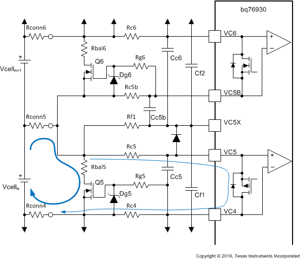
The timelines of the cell groups in the bq76930 and bq76940 are independent, so one group may be balancing while the next group is measuring. At the cell boundary between groups, the adjacent cell may measure a voltage from the balance current in any common path. Keeping the common path resistance low, using wide traces or returning the current as close to the cell as possible will reduce this effect (see Figure 8).
 Figure 8. Balancing at Group Boundary
 The system designer must determine how much balance current to provide. This is sometimes not an easy question. The self discharge rate of the cells may vary cell-to-cell, and with the environment in which they are operated. Cells which are at a higher temperature in the system may discharge faster. Where the cells and their environment are well matched, the electronics may contribute to an imbalance. The dINOM, dISHIP and dIALERT currents in the bq76930 and bq76940 will cause different loads on the cell groups and may eventually need to be balanced out. A pack which is charged every day may need lower balancing current than a pack which is charged monthly, or a pack which is charged infrequently may need to balance longer than a frequently charged pack when using the same balance current.