SLUAA93 November 2020 UCC28730-Q1
4 Pin Failure Mode Analysis (Pin FMA)
This section provides a Failure Mode Analysis (FMA) for the pins of the UCC28730-Q1. The failure modes covered in this document include the typical pin-by-pin failure scenarios:
- Pin short-circuited to Ground (see Table 4-2)
- Pin open-circuited (see Table 4-3)
- Pin short-circuited to an adjacent pin (see Table 4-4)
- Pin short-circuited to supply (see Table 4-5)
Table 4-2 through Table 4-5 also indicate how these pin conditions can affect the device as per the failure effects classification in Table 4-1.
| Class | Failure Effects |
|---|---|
| A | Potential device damage that affects functionality |
| B | No device damage, but loss of functionality |
| C | No device damage, but performance degradation |
| D | No device damage, no impact to functionality or performance |
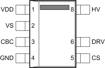
Figure 4-1 shows the UCC28730-Q1 pin diagram. For a detailed description of the device pins please refer to the Pin Configuration and Functions section in the UCC28730-Q1 data sheet.
 Figure 4-1 Pin Diagram
Following are the assumptions of use and the device configuration assumed for the pin FMA in this section:
- The UCC28730-Q1 is connected according to UCC28730-Q1 datasheet Figure 8-1 Simplified Application With Ground-Referenced Diode
- The VDD is considered as supply pin
| Pin Name | Pin No. | Description of Potential Failure Effect(s) | Failure Effect Class |
|---|---|---|---|
| VDD | 1 | Device is not function system will not startup. | B |
| VS | 2 | IC remains in input under voltage protection mode. The output of the Flyback converter remains at zero. | B |
| CBC | 3 | Cable compensation will be set at its highest value. | C |
| GND | 4 | No effect. | D |
| CS | 5 | When CS pin is shorted before the IC start-up, CS pin short protection. The output of the Flyback converter remains at zero. | B |
| When CS pin is shorted after the IC already in operation, DRV remains high. Potential power stage damage and it might cause IC damange. | A | ||
| DRV | 6 | DRV remains low. The output of the Flyback converter remains at zero. | B |
| N/A | 7 | ||
| HV | 8 | The VDD capacitor cannot be trickle charged and the converter will never startup. | B |
| Pin Name | Pin No. | Description of Potential Failure Effect(s) | Failure Effect Class |
|---|---|---|---|
| VDD | 1 | No positive supply applied to device, device is not functional. | B |
| VS | 2 | IC remains in input under voltage protection mode. The output of the Flyback converter remains at zero. | B |
| CBC | 3 | Cable compensation is reduced to It's minimal value. | C |
| GND | 4 | Device damage | A |
| CS | 5 | When CS pin is shorted before the IC start-up, CS pin short protection. The output of the Flyback converter remains at zero. | B |
| When CS pin is shorted after the IC already in operation, DRV remais high. Potential power stage damage and it might cause IC damange. | A | ||
| DRV | 6 | The output of the Flyback converter remains at zero. | B |
| N/A | 7 | ||
| HV | 8 | The VDD capacitor cannot be trickle charged. Output of the converter remains at zero volts. | B |
| Pin Name | Pin No. | Shorted to | Description of Potential Failure Effect(s) | Failure Effect Class |
|---|---|---|---|---|
| VDD | 1 | VS | VS max voltage rating exceeded, device damaged, possible Flyback switch damage | A |
| VS | 2 | CBC | Cable compensation will not be stable, output voltage will not regulate correctly | C |
| CBC | 3 | GND | Cable compensation will be set at its highest value. | C |
| GND | 4 | N/A | ||
| CS | 5 | DRV | CS max voltage rating will be exceeded, device damage, possible Flyback switch damage | A |
| DRV | 6 | N/A | ||
| N/A | 7 | N/A | ||
| HV | 8 | N/A |
| Pin Name | Pin No. | Description of Potential Failure Effect(s) | Failure Effect Class |
|---|---|---|---|
| VDD | 1 | No Effect. | D |
| VS | 2 | DRV remains low. Possible IC damage. | A |
| CBC | 3 | DRV remains low. Possible IC damage. | A |
| GND | 4 | No positive supply applied to device. Device is non-functional. | B |
| CS | 5 | DRV remains low. Possible IC damage. | A |
| DRV | 6 | DRV remains high. Possible IC damage and Flyback switch damage. | A |
| N/A | 7 | ||
| HV | 8 | The max rating of VDD will be exceeded, possible device damage and Flyback switch damage. | A |