SLUAAC5 August 2021 UCC28700 , UCC28701 , UCC28702 , UCC28703 , UCC28704 , UCC28710 , UCC28711 , UCC28712 , UCC28713 , UCC28720 , UCC28722 , UCC28730 , UCC28740 , UCC28742 , UCC28910 , UCC28911
- Trademarks
- 1 Introduction
- 2 Brief Review of DCM FM, AM, FM Flyback Control Law
- 3 Input (VIN) and Output (VOUT) Voltage Sensing for UVLO and OVP Fault Protection
- 4 Input Under Voltage Lockout (UVLO) Protection
- 5 Output Overvoltage (OVP) Protection
- 6 Not Recognizing a UVLO or OVP Fault
- 7 Separate Bias Supply Startup Issue and Resolution
- 8 Not Having a Clean Aux Winding Signal
- 9 Removing Aux Winding Ringing to Resolve False Triggering of OVP and UVLO Faults
- 10Noise on CS Pin Tripping Over Current Protection (OCP)
- 11Summary
- 12References
4 Input Under Voltage Lockout (UVLO) Protection
These flyback controllers have programmable input under voltage detection that can be set and adjusted primary to auxiliary turns ration and properly selecting RS1 and RS2Figure 1-1. Refer to the flyback controller data sheet for instructions on programming the input UVLO.
The VS pin of these flyback controllers have an internal clamp on the VS pin that clamps the VS pin to roughly ground (GND) while Q1 is on (tON), (Figure 3-1 and Figure 3-2). During this this time the current coming out of the VS pin (IVSL) in combination with RS1 and the NP/NA turns ratio will determine the input voltage level the flyback converter will start at (VIN(run)) and what input voltage the converter will stop switching at (VIN(stop)). The value IVSL(run) start and IVSL(stop) stop thresholds will vary based on the flyback controller that is used in the design, refer to the flyback controller data sheet for the correct values.
The design presented in Figure 1-1 does not start switching until VIN is greater than 67 V and will stop switching when VIN drops below 23.8 V. Refer to Equation 3 through Equation 6 for details.
When power is first applied to VIN the VDD capacitor (CDD) trickle charges through RT of Figure 1-1. Note that some flyback controllers trickle charge the CDD capacitor with an internal JFET startup circuit. The capacitor continues to trickle charge until the flyback controllers turn on threshold is reached (VVDD(on)). At this point it will deliver 3 gate drivers pulse to sample VIN and VOUT at the controllers maximum switching frequency (fSW(max)). The UCC28704 controls the primary current to IPP(max) /4. At this point tLK_RESET will be reduced to it's minimum blanking time of 750 ns. If the converter detects a UVLO and/or a OVP fault during this time, the gate driver stops switching and the IDD current will discharge CDD to the flyback controllers turnoff threshold (VVDD(off)). After CDD is discharged to VVDD(off), CDD will once again be charged through RT until the VDD pin reaches VVDD(on). At this point the controller will sample VOUT and VIN again. If the fault is cleared the flyback will continue to operate. If the fault is not cleared switching will stop and the CDD capacitor will be discharged and charged between VVDD(off) and VVDD(on) until the fault is cleared.
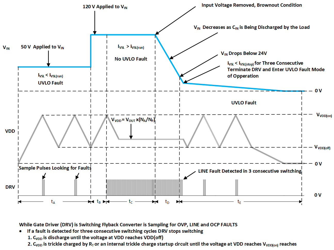
Figure 4-1, shows an example of how the input fault protection operates with different input voltages. At the beginning of time interval tA 50 V is applied at VIN, the CDD capacitor trickle charged up to VVDD(on). The flyback controller samples the input through NP/NA turns ratio and will detect an input UVLO fault and stops switching. The controller enters fault mode operation during this time interval. At the beginning of time interval tB the input voltage is increase to 120 V, however, the flyback controller is still not switching, it waits until CDD is charge up to VVDD(on) to gives three DRV pulses to sample the input voltage. At the beginning of time internal tC the flyback controller based on input sampling is no longer in a UVLO condition and the flyback converter will continue switching. The CDD capacitor will discharge down to the reflected output voltage determined by the NA/NS turns ratio, at this point the flyback controller will be powered by the auxiliary winding (NA) of T1. At the beginning of time interval tD the input voltage was removed from VIN simulating a brown out condition. The input bulk capacitor CIN discharges based on the loading on the output of the flyback converter. At the beginning of time interval tE capacitor CIN will have discharged to a point where the input voltage will cause a UVLO fault. The UVLO fault has to be sampled in three consecutive switching cycles before the flyback controller stop switching. The flyback controller will remain operating in this mode until an input voltage is applied to VIN that causes the IVLS current to be greater than IVSL(run).
 Figure 4-1 Example
of UVLO Fault Detection