SLUAAC5 August 2021 UCC28700 , UCC28701 , UCC28702 , UCC28703 , UCC28704 , UCC28710 , UCC28711 , UCC28712 , UCC28713 , UCC28720 , UCC28722 , UCC28730 , UCC28740 , UCC28742 , UCC28910 , UCC28911
- Trademarks
- 1 Introduction
- 2 Brief Review of DCM FM, AM, FM Flyback Control Law
- 3 Input (VIN) and Output (VOUT) Voltage Sensing for UVLO and OVP Fault Protection
- 4 Input Under Voltage Lockout (UVLO) Protection
- 5 Output Overvoltage (OVP) Protection
- 6 Not Recognizing a UVLO or OVP Fault
- 7 Separate Bias Supply Startup Issue and Resolution
- 8 Not Having a Clean Aux Winding Signal
- 9 Removing Aux Winding Ringing to Resolve False Triggering of OVP and UVLO Faults
- 10Noise on CS Pin Tripping Over Current Protection (OCP)
- 11Summary
- 12References
10 Noise on CS Pin Tripping Over Current Protection (OCP)
To help protect the FET from damage, these flyback controllers have an over current protection (OCP) circuit that trips when the CS pin senses a current sense signal that is 2X the nominal peak. In the case of the UCC28704 this OCP trip point is 1.5 V.
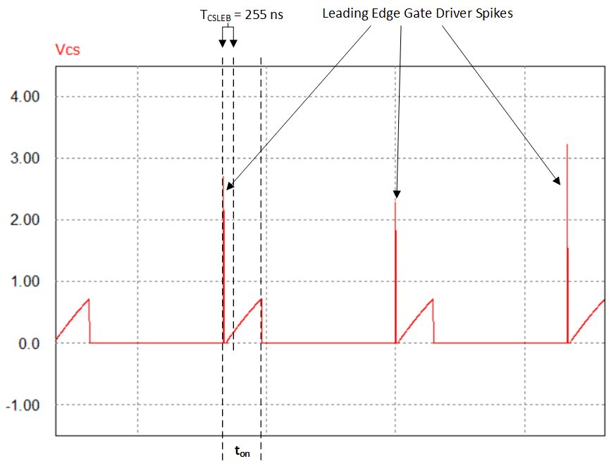
When first turning on a FET there is a leading-edge current spike caused by the charging the gate to source capacitance of the FET used in the design. This generally can be seen on the current sense signal (VCS), please refer to Figure 10-1 for details. To prevent the controller from falsely tripping OCP due to this leading-edge gate driver spike the flyback controller uses current sense leading edge blanking. The flyback controller will not sense the current sense signal during a predetermined blanking time (TCSLEB). In this example, the UCC28704 was evaluated and had a TCSLEB of 255 ns. Please note this time will vary based on flyback controller that is used in the design.
 Figure 10-1 CS
Leading Edge Blanking Helps Prevent False OCP Shutdown
Figure 10-1 CS
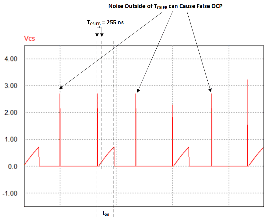
Leading Edge Blanking Helps Prevent False OCP ShutdownThese flyback designs sometimes shut down due to noise on the CS pin (VCS). This behaivor is not related to OVP or input UVLO sensing. This occurs by noise being coupled into the circuit through parasitic capacitance and/or poor layout. The problem occurs if these noise spikes are outside the TCSLEB blanking window and are larger than the OCP trip point. Please refer to Figure 10-2 for details.
 Figure 10-2 Noise Spikes Outside the
TCSLEB Window will Cause a False OCP Fault
Figure 10-2 Noise Spikes Outside the
TCSLEB Window will Cause a False OCP FaultA poor PCB layout can cause this fault as well. It is recommended to avoid this that the designer fallow the layout guidelines given in the TI flyback controller data sheets.
As an alternative, these noise spikes can be removed by using a low pass RC filter formed by RLC and CS presented in Figure 1-1. Resistor RLC is selected based on data sheet requirements and filter capacitor CS sets the pole of the low pass filter that can be adjusted. Select CS to put the filter pole at 10 times the converters maximum frequency. Equation 24 can be used to calculate CS. Please note if the flyback was designed for a maximum frequency of 75 kHz and had an RLC resistor of 1 k ohm it would require a CS of roughly 212 pF for snubbing.