SLUAAF9 September 2021 UCC28782
- Trademarks
- 1 Initial Board Visual Inspection and Start-up Check
- 2 Typical System Operating Waveforms
- 3Typical System Protection Waveforms
- 4Common Issues and Solutions
- 5References
3.3 Output Short-Circuit Protection (SCP)
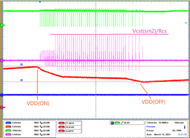
For SCP, VDD voltage needs to drop to VDD(OFF), the auxiliary winding voltage can reflects output voltage. If output been shorted, the AUX winding voltage during PWMH on time is also been clamped to a low voltage. Then UCC28782 internal current threshold (VCST) can reflect the VS pin voltage at Vvs (sm2). This can be reflected by capturing transformer primary winding current which equal to VVS(SM2) divide current sense resistor Rcs. CH4 in Figure 3-6 shows VS pin is at VVS(SM2) stage.
 Figure 3-6 SCP Delay to Action
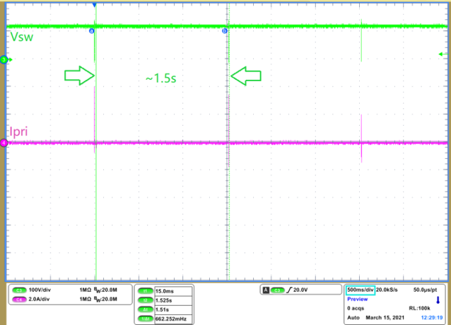
 Figure 3-7 SCP Action
CH3: Low side FET Vds, CH4: Primary current, CH2: VDD
Additional protections details and corresponding solutions can be found in Debugging UCC28780 ACF Converter Start-up Issues. application note.