SLUAAG2 October 2021 UCC28782
4.3 RTZ Pin (Sets Delay for Transition Time to Zero)
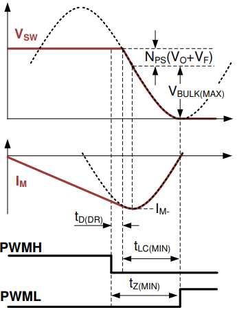
The dead-time between PWMH falling edge and PWML rising edge (tz) serves as the wait time for VSW transition from its high level down to the target ZVS point. Since the optimal tZ varies with VBULK, the internal dead-time optimizer automatically extends tz as VBULK is less than the highest voltage of the input bulk capacitor (VBULK(MAX)). The circulating energy for ZVS can be further reduced, obtaining higher efficiency at low line versus a fixed dead-time over a wide line voltage range. A resistor on the RTZ pin (RRTZ) programs the minimum tZ (tZ(MIN)) at VBULK(MAX), which is the sum of the propagation delay of the high-side driver (tD(DR)) and the minimum resonant transition time of VSW falling edge (tLC(MIN)).
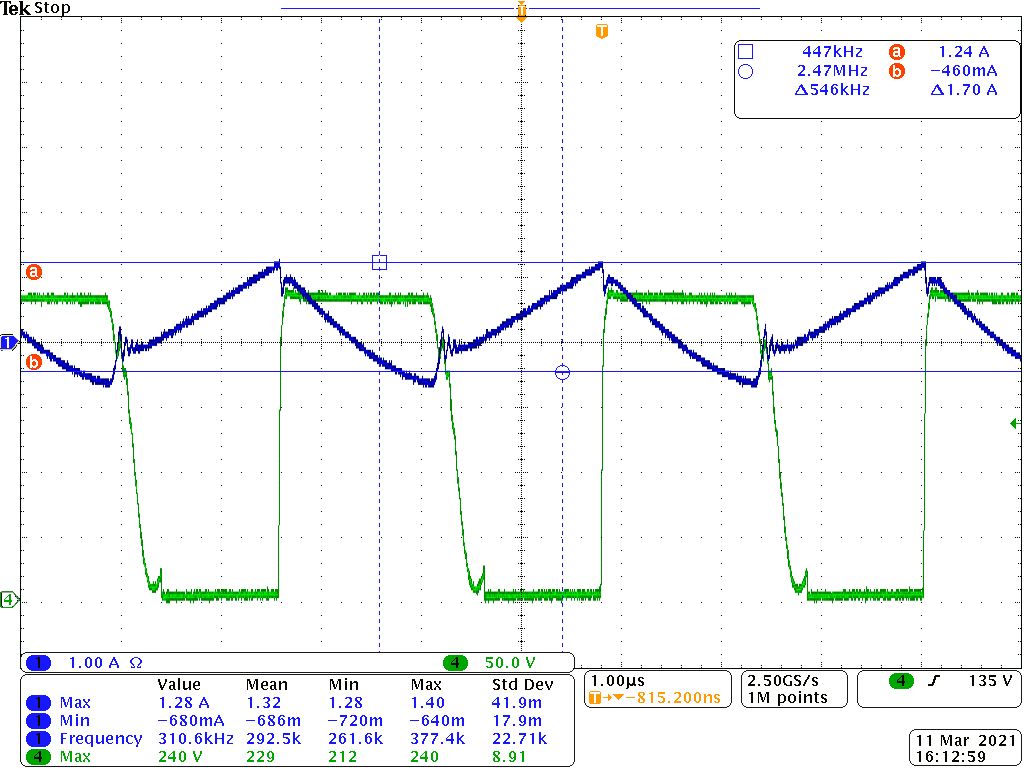
Normally the RTZ is designed as calculator result. If the VDS voltage has ring back voltage as Figure 4-3 showing, you need to reduce the RTZ resistance.
 Figure 4-3 RTZ Setting for the
Falling-edge Transition of VSW
 Figure 4-4 RTZ Setting too large cause
VDS ring back