SLUAAJ7 June   2022 UCC256402 , UCC256403 , UCC256404


  1.   Abstract
  2.   Trademarks
  3. 1UCC25640x Selection Guide
  4. 2UCC25640x Features Brief Overview
    1. 2.1 High Voltage(HV) Startup
      1. 2.1.1 HV Startup Procedure
      2. 2.1.2 HV Startup with External Bias
      3. 2.1.3 HV Start-up, VCC, X-cap Discharge Internal Block Diagram
      4. 2.1.4 HV Startup External Resistor
    2. 2.2 XCAP Discharge
      1. 2.2.1 IEC Standards
      2. 2.2.2 Detecting AC presence
      3. 2.2.3 Test Current Injection for Zero Crossing Detection
      4. 2.2.4 Typical Waveforms of HV Startup and XCAP Discharge
    3. 2.3 Feedback Chain
      1. 2.3.1 FBreplica Generation
      2. 2.3.2 Vcomp Signal and Threshold Voltages
      3. 2.3.3 FB Pin Voltage Typical Waveform at no Load
    4. 2.4 Hybrid Hysteretic Control and VCR Pin Voltage and Gate Pulse Generation
      1. 2.4.1 Hybrid Hysteretic Control
      2. 2.4.2 VCR Pin Voltage
      3. 2.4.3 VCR Typical Waveform
    5. 2.5 Soft Start
      1. 2.5.1 Soft Start Timing
      2. 2.5.2 Soft Start Initial Voltage Programming
    6. 2.6 Burst Mode
      1. 2.6.1 Burst Patterns
      2. 2.6.2 BMTL/BMTH Ratio Programming
      3. 2.6.3 BMTH Generation
      4. 2.6.4 Interpreting BMTL and BMTH
      5. 2.6.5 Soft On or Off
      6. 2.6.6 Operation when Burst Mode Disabled
      7. 2.6.7 Typical Waveforms
    7. 2.7 Adaptive Dead Time Control
    8. 2.8 Fault Management
      1. 2.8.1 OCP Protection
      2. 2.8.2 OCP Fault Typical Waveforms
      3. 2.8.3 Over Voltage Protection using Bias Winding (BW OVP)
      4. 2.8.4 Restart or Latch
    9. 2.9 ZCS Region Prevention Scheme
      1. 2.9.1 ZCS Effects
      2. 2.9.2 ZCS Detection and Prevention and Disabling
  5. 3UCC25640x Power Up Guidelines and Debugging Notes
    1. 3.1  Power Up Procedure
    2. 3.2  HV Pin
    3. 3.3  VCC Pin
    4. 3.4  BLK Pin
    5. 3.5  FB Pin
    6. 3.6  ISNS Pin
    7. 3.7  VCR Pin
    8. 3.8  BW Pin
    9. 3.9  LL/SS Pin
    10. 3.10 LO Pin
    11. 3.11 RVCC Pin
    12. 3.12 HS, HO, HB Pins
  6. 4References

BMTL/BMTH Ratio Programming

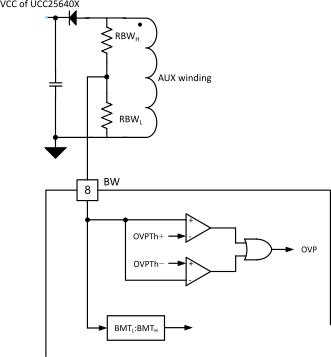
GUID-20220531-SS0I-DVQQ-HFWD-1FQWTTVWPNTP-low.png Figure 2-27 Internal Diagram and Typical Circuit of BW Pin of UCC25640X
Equation 8. GUID-20220531-SS0I-CWPH-XRDN-HG72XLPL5HFK-low.png
  • BW pin is multiplex for BMTL/BMTH ratio programming and Over voltage protection (OVP). This pin sources a fixed current of 54 uA before soft start to determine the BW voltage and it is internally compared with a series of voltage levels to determine the BMTL/BMTH ratio. It would take 2 ms to determine this BW pin voltage.
  • In case if the capacitor is connected the BW pin to eliminate the high frequency noise, its value should be such that time constant of RBW and CBW much less than 2 ms of the proper programming.
  • Based on the BW pin equivalent resistance (RBW value as given in Equation 8), the ratio of BMTL and BMTH is determined as shown in the Table 2-1
Table 2-1 BMTL/BMTH value
Option RBW BMTL/BMTH
1 > 24.7 k 0.95
2 17.1 k – 19.9 k 1
3 12.5 k – 13.6 k 0.9
4 9.02 k – 9.81 k 0.8
5 6.48 k – 6.85 k 0.6 (No Vssinit)
6 4.45 k – 4.73 k 0.6
7 2.42 k – 3.04 k 0.4 (Burst disabled)
8 Shorted 0.6