SLUP408 February 2022 LM25149-Q1 , LM61460-Q1 , LM61495-Q1 , LMQ61460-Q1
- 1 Introduction
- 2 Defining EMI
- 3 What Causes EMI in a Switched-Mode DC/DC Regulator?
- 4 Existing Passive EMI Filtering Techniques
- 5 Passive Filter Limitations
- 6 AEF
- 7 Spread Spectrum
- 8 DRSS
- 9 True Slew-Rate Control
- 10HotRod™ Package Technology
- 11Optimized Package and Pinout
- 12Integrated Capacitors
- 13Conclusions
- 14References
- 15Important Notice
4 Existing Passive EMI Filtering Techniques
Figure 4-1 illustrates how to mitigate and filter EMI with passive components.
 Figure 4-1 Typical input filter
components.
Figure 4-1 Typical input filter
components.A high-frequency ceramic input capacitor helps supply the power metal-oxide semiconductor field-effect transistors (MOSFETs) with high-frequency energy to improve the switch’s slew-rate and edge characteristics, thus reducing switch ringing and high-frequency noise. Bulk capacitance provides low-frequency damping and prevents resonance between the filter components. A capacitor-inductor-capacitor (CLC) EMI filter, also known as a π filter, filters differential-mode noise from 10 MHz to 100 MHz, depending on the components selected.
Other components include a ferrite bead that provides high differential-mode impedance at very high frequencies. The ferrite bead impedance is typically specified at 100 MHz. A common-mode choke filters common-mode noise that usually occurs at high frequencies (10 MHz to 300 MHz).
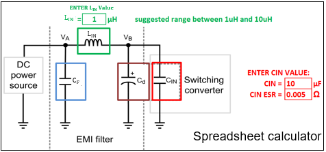
Conventional CLC EMI filters use a capacitor and inductor arranged as a low-pass filter to attenuate noise from a noisy node to a quiet node. You can design the CLC components based on the required attenuation. Many tools are available to aid in designing filters, including application notes [2] and spreadsheet tools [3], as shown in Figure 4-2.
 Figure 4-2 Input filter calculator Excel
tool for designing a CLC EMI filter.
Figure 4-2 Input filter calculator Excel
tool for designing a CLC EMI filter.Alternatively, you could use Equation 1 to measure or estimate the required attenuation:
where fSW is the switching frequency, CIN is the input capacitance, D is the duty cycle, IDC is the converter-inductor DC current and VMAX is the decibel microvolt (dBµV) limit at the switching frequency.
Looking again at Figure 4-2 and considering the filter inductor (LIN) and filter capacitor (CF), the CLC π filter provides 40 dB of attenuation per decade at frequencies above the cutoff frequency. Figure 3-1 takes the attenuation required at the switching frequency to design the π-filter cutoff frequency:
You can then use Equation 3 to select filter components based on the required cutoff frequency:
After selecting a typical LIN range between 0.1 µH and 10 µH, you can calculate the required CF value. Increasing the capacitance value – as opposed to using larger inductance values, since a larger inductance tends to increase the overall filter size – lowers the cutoff frequency. Plus, higher-value inductors tend to have decreased current ratings for a given size. The most space-efficient designs use more parallel capacitors rather than a larger inductor value.
Increasing CF capacitance with multiple parallel capacitors is usually easier and more space-effective than increasing LIN to adjust the filter cutoff frequency. Furthermore, a higher inductance will have a decreased current rating for given size.