SLUP412 February 2022 LMG3522R030-Q1
- 1 Introduction
- 2 Comparing Different Technologies
- 3 Advantages of Integrating the Driver With GaN FETs
- 4 The GaN-Based 6.6-kW OBC Reference Design
- 5 PFC Stage
- 6 DC/DC Stage
- 7 DC/DC Topology Selection
- 8 Frequency Selection
- 9 Core Loss
- 10Loss of ZVS
- 11Dead Time
- 12ISR Bandwidth
- 13Overall
- 14Resonant Tank Design
- 15Thermal Solution
- 16Layout Best Practices
- 17Control-Loop Considerations
- 18Conclusions
- 19References
- 20Important Notice
16 Layout Best Practices
As the power density increases, an optimal layout becomes even more important in order to guarantee a low noise floor and good signal integrity. In addition, GaN FETs have a much higher switch-node transient voltage (dv/dt) than silicon or SiC. Preventing dv/dt from coupling unwanted noise into sensitive nodes requires careful layout planning.
The first step in a high-quality layout is to ensure that the GaN FETs have a low inductance decoupling loop in order to minimize switching losses and minimize VDS overshoot. Without this, excessive ringing on the drain-to-source can negatively impact stability, signal integrity and EMI.
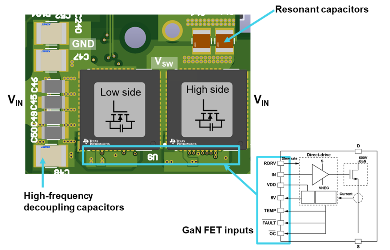
Figure 16-1 shows the layout of one of the CLLLC’s half bridges that uses a vertically oriented switching loop with high-frequency decoupling capacitors on the left, a low-side GaN FET in the center, a high-side GaN FET on the right, and two resonant capacitors above the high-side GaN FET.
 Figure 16-1 GaN FET PWB component
placement and decoupling.
Figure 16-1 GaN FET PWB component
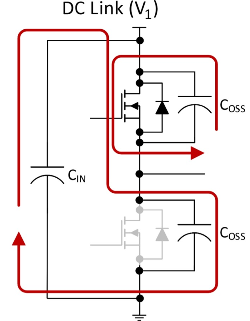
placement and decoupling.In order to visualize the benefits of this layout, Figure 16-2 shows the conduction paths when the high-side device turns on with hard switching. The fast rate at which these switches turnon and off results in very large transient currents (di/dt). If these conduction paths have an appreciable inductance, excessive voltage spikes will occur.
 Figure 16-2 Schematic of hard-switching
turnon current-loop conduction path.
Figure 16-2 Schematic of hard-switching
turnon current-loop conduction path.Equation 8 estimates the inductance:
where µ0 is the permeability of free space ( ), µr is the relative permeability (in this case, 1), N is the number of turns (in this case, one), Ae is the area of the conduction path and Ie is the magnetic path length.
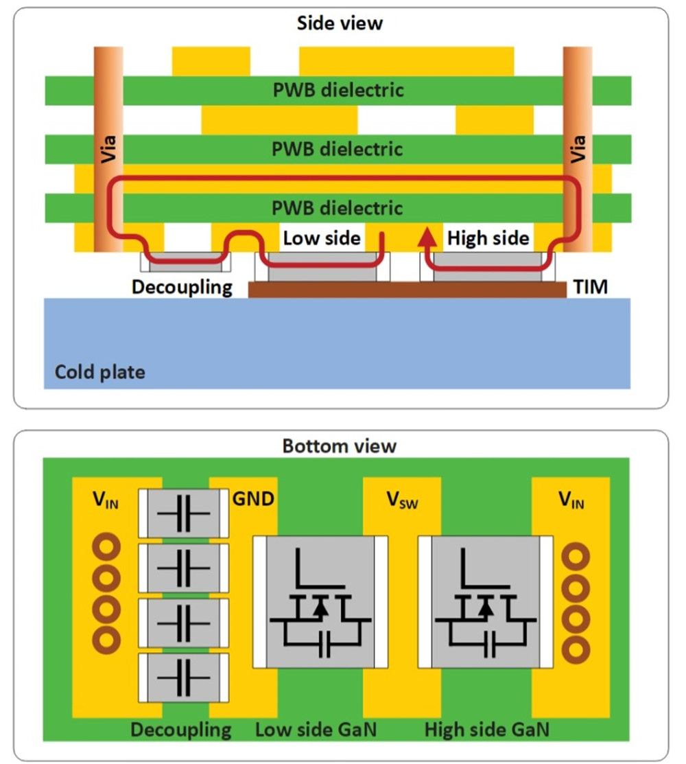
Figure 16-3 is a simplified cross-section of the PWB bottom-side components, with the hard-switching turnon edge-conduction current shown in red. The vertical scale of the image was exaggerated to make it easier to see; in reality, the total board thickness is about 90 mils. Notice that the loop created by the current has a very small area, which implies that the inductance is very small, as shown in Equation 8.
 Figure 16-3 Simplified low-inductance
decoupling loop: views from the side (top) and above (bottom).
Figure 16-3 Simplified low-inductance
decoupling loop: views from the side (top) and above (bottom).Figure 16-4 shows the actual bottom-side component placement and routing for layer 8. This placement and routing reflects the same concept for the power loop illustrated in Figure 16-3. Red indicates the switch node, green indicates the primary-side ground, blue is the DC link, and gray indicates the different input signals to the GaN FETs. The cold plate electrically connects to ground.
None of the signals shown on the snippet of layer 8 are equal to the voltage potential of the cold plate. Essentially, the cold plate acts as one side of a large capacitor. Since the GaN FET switch nodes create very large dv/dt, minimizing the influence of this parasitic capacitance must be a priority. Extra capacitance on the switch node will slow down the switching transition and create more losses.
Additionally, all of the inputs of the high-side GaN FET are referenced to the switch node, which means that they experience the same dv/dt with respect to ground and the cold plate.
There are no components on the bottom side associated with the GaN FET inputs. There are also minimal copper features on the inputs so as to avoid any coupling to the cold plate that might induce noise.
Layer 7 provides the power-loop decoupling return path from Figure 16-3, shown in blue. Adding a shield protects any coupling to pins and traces on layer 8. This shield also protects the vias on layer 7 from noise coupling to the input voltage plane.
Layer 6 creates a void in the same location of layer 7’s shield to prevent capacitive coupling to the inputs.
 Figure 16-4 GaN half-bridge layout –
bottom-side considerations.
Figure 16-4 GaN half-bridge layout –
bottom-side considerations.Figure 16-5 shows the top-side features, with sensitive components and traces added to the top of the PWB. Keeping these components within a small area avoids any additional noise coupling. Layer 2 is used for interconnect, while layer 3 contains another shield to protect the components and traces on layers 1 and 2 from noisy signals not referenced to the switch node.