SLUS515G September 2002 – December 2015 UCC28050 , UCC28051 , UCC38050 , UCC38051
PRODUCTION DATA.
- 1 Features
- 2 Applications
- 3 Description
- 4 Revision History
- 5 Pin Configuration and Functions
- 6 Specifications
- 7 Detailed Description
- 8 Application and Implementation
- 9 Power Supply Recommendations
- 10Layout
- 11Device and Documentation Support
- 12Mechanical, Packaging, and Orderable Information
8 Application and Implementation
NOTE
Information in the following applications sections is not part of the TI component specification, and TI does not warrant its accuracy or completeness. TI’s customers are responsible for determining suitability of components for their purposes. Customers should validate and test their design implementation to confirm system functionality.
8.1 Application Information
The UCC38050 and UCC38051 are switch-mode controllers used in boost converters for power factor correction operating in transition mode. In the transition mode operation, the PWM circuit is self-oscillating, with the turnon being governed by an inductor zero-current detector (ZCD pin), and the turnoff being governed by the current-sense comparator. Additionally, the controller provides features such as peak current limit, default timer, OVP, and enable.
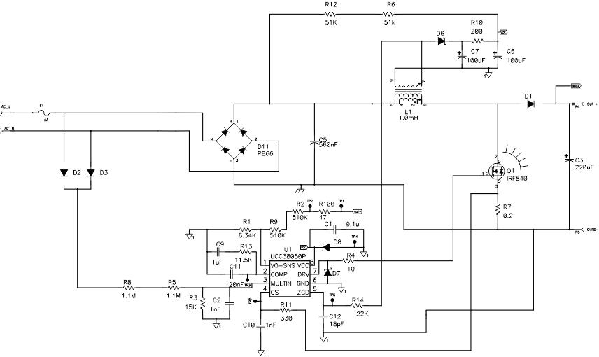
There are two key parametric differences between UCC38050 and UCC38051. The UVLO turnon threshold of UCC38050 is 15.8 V, while for UCC38051 it is 12.5 V. Secondly, the gM amplifier source current for UCC38050 is typically 1.3 mA, while for UCC38051 it is 300 μA. The UCC38051 is suitable for multiple applications, including AC adapters, where a two-stage power conversion is needed. The UCC38050 is suitable for applications such as electronic ballasts, where there is no down-stream PWM conversion and the advantages of a smaller VCC capacitor and improved transient response can be realized. Figure 19 is an example of a critical conduction mode power factor correction boost converter utilizing the UCC38050.
8.2 Typical Application
The UCC38050 is used for the off-line power factor corrected pre-regulator with operation over a universal input range of 85 V to 265 V with a 400-VDC regulated output. The schematic is shown in Figure 19, and the board layout for the reference design is shown in Figure 24.
 Figure 19. Universal Line Input 100-W Boost Converter
 Figure 20. Typical Application Diagram
8.2.1 Design Requirements
Table 1 shows the design requirements for a CCM, PFC boost converter utilizing the UCC38050.
Table 1. UCC38050 Design Requirements
| PARAMETER | TEST CONDITION | MIN | TYP | MAX | UNIT | |
|---|---|---|---|---|---|---|
| VIN | Input voltage | 85 | 265 | VRMS | ||
| Input frequency | 60 | Hz | ||||
| VOUT | Output voltage DC | VIN = 85 VRMS | 370 | 400 | 425 | V |
| VOUT | Output voltage DC | VIN = 265 VRMS | 370 | 390 | 410 | V |
| POUT | Output power | 0 | 100 | W | ||
| Output voltage ripple | VIN = 85 VRMS | 3% | ||||
| Efficiency | POUT = 100 W | 90% | ||||
| Total harmonic distortion (THD) | VIN = 85 VRMS, POUT = 100 W | 5% | ||||
| Total harmonic distortion (THD) | VIN = 265 VRMS, POUT = 100 W | 15% | ||||
| Hold-up time | 16.7 | ms | ||||
8.2.2 Detailed Design Procedure
For a selected VOUT and minimum switching frequency, the following equations outline the design guidelines for power stage component selection, using a universal input, 100-W PFC converter with an output voltage of 390 V. Refer to Figure 20 for reference designators.
8.2.2.1 Inductor Selection
In the transition mode control, the inductor value must be calculated to start the next switching cycle at zero current. The time it takes to reach zero depends on line voltage and inductance and as shown in Equation 2. L determines the frequency range of the converter.

where
- VAC = RMS line voltage
- VAC(min) = minimum AC line voltage
- PIN = maximum input power averaged over the ac line period
8.2.2.2 MOSFET Selection
The main switch selection is driven by the amount of power dissipation allowable. Choose a device that minimizes gate charge and capacitance, and minimizes the sum of switching and conduction losses at a given frequency.

8.2.2.3 Diode Selection
The effects of the reverse recovery current in the diode can be eliminated with relatively little negative impact to the system. The diode selection is based on reverse voltage, forward current, and switching speed.

8.2.2.4 Capacitor Selection
The hold-up time is the main requirement in determining the output capacitance. ESR and the maximum RMS ripple current rating can also be important, especially at higher power levels.
where
- VOUT(min) = minimum regulator input voltage for operation

8.2.2.5 Multiplier Set-Up
Select RAC1 and RAC2 so that their ratio uses the full dynamic range of the multiplier input at the peak line voltage, and yet with values small enough to negate the effects of the multiplier bias current. To use the maximum range of the multiplier, select the divider ratio so that VMULTIN, evaluated at the peak of the maximum ac line voltage, is the maximum of the minimum dynamic input range of MULTIN, which is 2.5 V. Choose RAC1 so that it has at least 100 μA at the peak of the minimum AC operating line voltage.

In extreme cases, switching transients can contaminate the MULTIN signal, so it can be beneficial to add capacitor CAC1. Select the value of CAC1 so that the corner frequency of the resulting filter is greater than the lowest switching frequency. The low corner frequency of this filter may compromise the overall power factor.
8.2.2.6 Sense Resistor Selection
The current sense resistor value must be chosen to limit the output power, and it must also use the full dynamic range of the multiplier during normal steady state operation. The value of RS1 is thus selected for maximum power operation at low ac line voltage conditions. To use the full dynamic range, set the VSENSE threshold as a function of the dynamic input range of VCOMP and the peak of the minimum MULTIN voltage.

where
- COMP(MAX) = 3.8 V
- COMP(MIN) = 2.5 V
- MULTIN(PEAK)@VAC(min) = √2 × VAC(min)( RAC2 / (RAC2+RAC1) )
If the exact value RS1 is not available, RS2 and RS3 can be added for further scaling. The CS pin already has an internal filter for noise due to switching transients. Additional filtering at switching transient frequencies can be achieved by adding CS1.
8.2.2.7 Output Voltage Sense Design
Select the divider ratio of RO1 and RO2 to set the VO_SNS voltage to 2.5 V at the desired output voltage. The current through the divider should be at least 200 μA.
8.2.2.8 Voltage Loop Design
How well the voltage control loop is designed directly impacts line current distortion. UCC38050 employs a transconductance amplifier (gM amp) with gain scheduling for improved transient response (refer to Figure 9). Integral type control at low frequencies is preferred, because the loop gain varies considerably with line conditions. The largest gain occurs at maximum line voltage. If the power factor corrector load is dc-to-dc switching converter, the small signal model of the controller and the power factor corrector, from COMP to PFC output voltage is given by:

where
- ^VOUT = small signal variations in VOUT
- ^VCOMP = small signal variations in VCOMP
- k1 = multiplier gain = 0.65
- kCRM = peak to average factor = 2
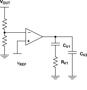
A controller that has integral control at low frequencies requires a zero near the crossover frequency to be stable. The resulting gM amplifier configuration is shown in Figure 21.
 Figure 21. gM Amplifier Configuration
The compensator transfer function is:

where
- gM = DC transconductance gain = 100 μs
The limiting factor of the gain is usually the allowable third harmonic distortion, although other harmonics can dominate. The crossover frequency of the control loop will be much lower than twice the AC line voltage. To choose the compensator dynamics, determine the maximum allowable loop gain at twice the line frequency, and solve for capacitor CV2. This also determines the crossover frequency.


Select CV1 so that the low frequency zero is one-tenth of the crossover frequency.
Select RV1 so that the pole is at the crossover frequency.
8.2.3 Application Curves
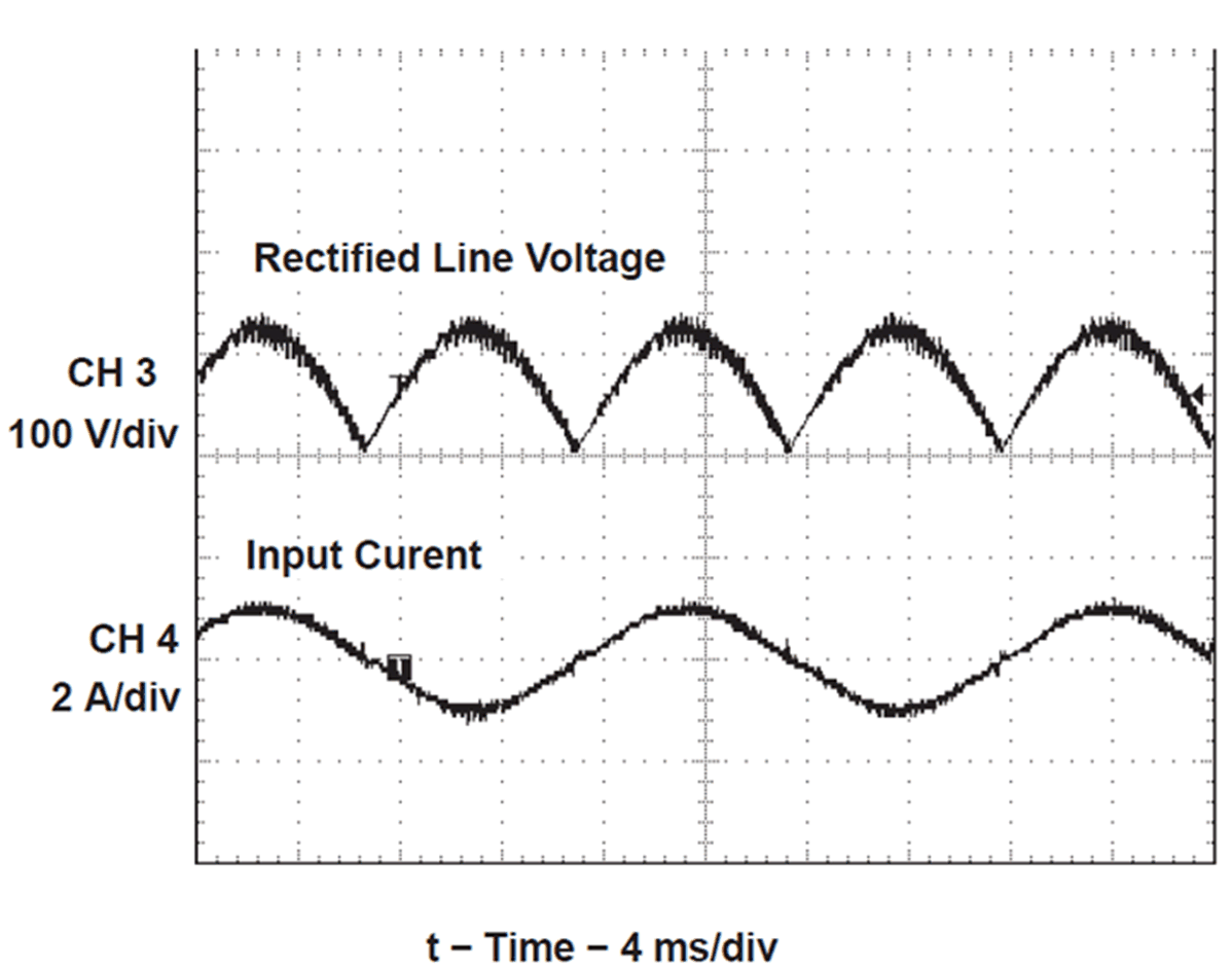
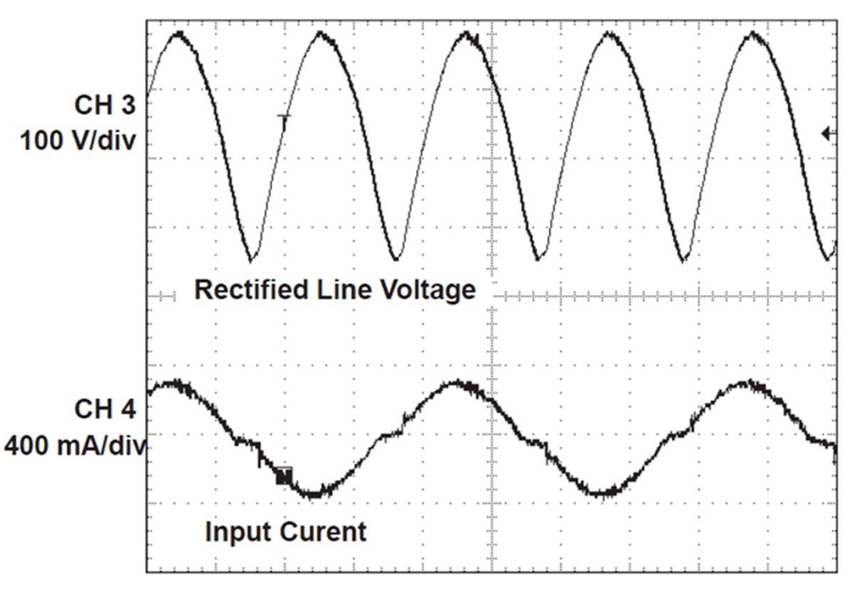
Figure 22 and Figure 23 show the input current and rectified line for the power module.
- Channel 3 = Rectified Line Voltage
- Channel 4 = Power Module Input Current

| VIN = 85 V | POUT = 100 W |

| VIN = 265 V | POUT = 100 W |