SLUS515G September 2002 – December 2015 UCC28050 , UCC28051 , UCC38050 , UCC38051
PRODUCTION DATA.
- 1 Features
- 2 Applications
- 3 Description
- 4 Revision History
- 5 Pin Configuration and Functions
- 6 Specifications
- 7 Detailed Description
- 8 Application and Implementation
- 9 Power Supply Recommendations
- 10Layout
- 11Device and Documentation Support
- 12Mechanical, Packaging, and Orderable Information
6 Specifications
6.1 Absolute Maximum Ratings
over operating free-air temperature range (unless otherwise noted)(1)| MIN | MAX | UNIT | ||
|---|---|---|---|---|
| Supply voltage, VCC | (Internally clamped) | 20 | V | |
| Input current into VCC clamp | IDD | 30 | mA | |
| Input current | ZCD | ±10 | mA | |
| Gate drive current (peak), IDRV | DRV | ±750 | mA | |
| Input voltage, VCC | VO_SNS, MULTIN, CS | 5 | V | |
| Maximum negative voltage | VO_SNS, MULTIN, DRV, CS | –0.5 | V | |
| Power dissipation at TA = 50°C | D package | 650 | mW | |
| P package | 1 | W | ||
| Operating junction temperature range, TJ | –55 | 150 | °C | |
| Storage temperature, Tstg | –65 | 150 | °C | |
| Lead temperature 1,6 mm (1/16 inch) from case for 10 seconds | 300 | °C | ||
(1) Stresses beyond those listed under Absolute Maximum Ratings may cause permanent damage to the device. These are stress ratings only, which do not imply functional operation of the device at these or any other conditions beyond those indicated under Recommended Operating Conditions. Exposure to absolute-maximum-rated conditions for extended periods may affect device reliability.
6.2 ESD Ratings
| VALUE | UNIT | |||
|---|---|---|---|---|
| SOIC PACKAGE | ||||
| V(ESD) | Electrostatic discharge | Human-body model (HBM), per ANSI/ESDA/JEDEC JS-001(1) | ±2000 | V |
| Charged-device model (CDM), per JEDEC specification JESD22-C101(2) | ±500 | V | ||
(1) JEDEC document JEP155 states that 500-V HBM allows safe manufacturing with a standard ESD control process.
(2) JEDEC document JEP157 states that 250-V CDM allows safe manufacturing with a standard ESD control process.
6.3 Recommended Operating Conditions
over operating free-air temperature range (unless otherwise noted)| MIN | NOM | MAX | UNIT | ||
|---|---|---|---|---|---|
| VCC input voltage from a low-impedance source | VCCOFF + 1 V | 18 | V | ||
| Operating junction temperature, TJ | –40 | 125 | °C | ||
6.4 Thermal Information
| THERMAL METRIC(1) | UCC2805x, UCC3805x | UNIT | ||
|---|---|---|---|---|
| D (SOIC) | P (PDIP) | |||
| 8 PINS | 8 PINS | |||
| RθJA | Junction-to-ambient thermal resistance | 113.6 | 55.6 | °C/W |
| RθJC(top) | Junction-to-case (top) thermal resistance | 60.3 | 45.5 | °C/W |
| RθJB | Junction-to-board thermal resistance | 54.3 | 32.7 | °C/W |
| ψJT | Junction-to-top characterization parameter | 14 | 23.1 | °C/W |
| ψJB | Junction-to-board characterization parameter | 53.8 | 32.6 | °C/W |
(1) For more information about traditional and new thermal metrics, see the Semiconductor and IC Package Thermal Metrics application report, SPRA953.
6.5 Electrical Characteristics
TA = 0°C to 70°C for the UCC3805x, –40°C to +105°C for the UCC2805x, TA = TJ, VCC = 12 V.| PARAMETER | TEST CONDITIONS | MIN | TYP | MAX | UNIT | ||
|---|---|---|---|---|---|---|---|
| SUPPLY | |||||||
| VCC operating voltage | 18 | V | |||||
| Shunt voltage | IVCC = 25 mA | 18 | 19 | 20 | V | ||
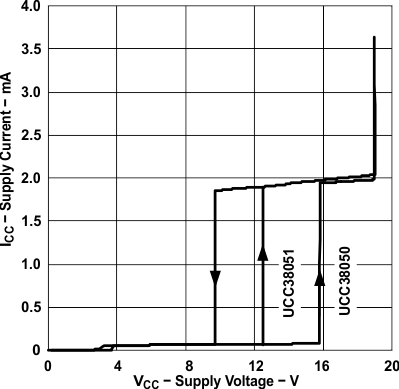
| Supply current, off | VCC = VCC turnon threshold –300 mV | 75 | 125 | µA | |||
| Supply current, disabled | VO_SNS = 0.5 V | 2 | 4 | mA | |||
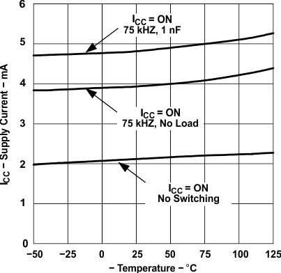
| Supply current, on | 75 kHz, CL = 0 nF | 4 | 6 | mA | |||
| Supply current, dynamic operating | 75 kHz, CL = 1 nF | 5 | 7 | mA | |||
| UVLO | |||||||
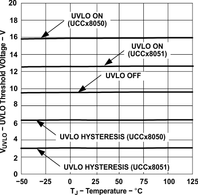
| VCC turnon threshold | UCCx8050 | 15.4 | 15.8 | 16.4 | V | ||
| UCCx8051 | 12 | 12.5 | 13 | ||||
| VCC turnoff threshold | 9.4 | 9.7 | 10 | V | |||
| UVLO hysteresis | UCCx8050 | 5.8 | 6.3 | 6.8 | V | ||
| UCCx8051 | 2.3 | 2.8 | 3.3 | ||||
| VOLTAGE AMPLIFIER (VO_SNS) | |||||||
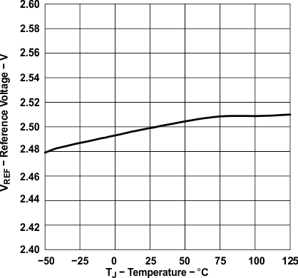
| Input voltage (VREF) | UCC3805x | 2.46 | 2.5 | 2.54 | V | ||
| UCC2805x | 2.45 | 2.5 | 2.55 | ||||
| Input bias current | 0.5 | µA | |||||
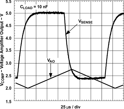
| VCOMP high | VO_SNS = 2.1 V | 4.5 | 5.5 | V | |||
| VCOMP low | VO_SNS = 2.55 V | 1.8 | 2.45 | V | |||
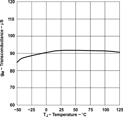
| gM | TJ = 25 °C, VCOMP = 3.5 V | 60 | 90 | 130 | µS | ||
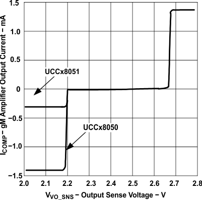
| Source current | UCCx8050 | VO_SNS = 2.1 V, VCOMP = 3.5 V | –0.2 | –0.1 | mA | ||
| UCCx8051 | VO_SNS = 2.1 V, VCOMP = 2.5 V | –200 | –300 | –400 | µA | ||
| Sink current | VO_SNS = 2.7 V, VCOMP = 3.5 V | 0.2 | 1 | mA | |||
| OVER VOLTAGE PROTECTION / ENABLE | |||||||
| Overvoltage reference | UCCx8050 | VREF + 0.165 | VREF + 0.19 | VREF + 0.21 | V | ||
| UCCx8051 | VREF + 0.15 | VREF + 0.18 | VREF + 0.21 | ||||
| Hysteresis | UCCx8050 | 175 | 200 | 225 | mV | ||
| UCCx8051 | 150 | 180 | 210 | ||||
| Enable threshold | UCCx8050 | 0.62 | 0.67 | 0.72 | V | ||
| UCCx8051 | 0.18 | 0.23 | 0.28 | ||||
| Enable hysteresis | 0.05 | 0.1 | 0.2 | V | |||
| MULTIPLIER | |||||||
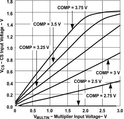
| Multiplier gain constant (k) | VMULTIN = 0.5 V, COMP = 3.5 V | 0.43 | 0.65 | 0.87 | 1/V | ||
| Dynamic input range, VMULTIN INPUT | 0 to 2.5 | 0 to 3.5 | V | ||||
| Dynamic input range, COMP INPUT | 2.5 to 3.8 | 2.5 to 4 | V | ||||
| Input bias current, MULTIN | 0.1 | 1 | µA | ||||
| ZERO POWER | |||||||
| Zero power comparator threshold(1) | Measured on VCOMP | 2.1 | 2.3 | 2.5 | V | ||
| ZERO CURRENT DETECT | |||||||
| Input threshold (rising edge)(1) | 1.5 | 1.7 | 2 | V | |||
| Hysteresis(1) | 250 | 350 | 450 | mV | |||
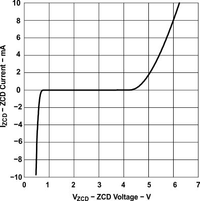
| Input high clamp | I = 3 mA | 5 | 6 | V | |||
| Input low clamp | I = −3 mA | 0.3 | 0.65 | 0.9 | V | ||
| Restart time delay | 200 | 400 | µs | ||||
| CURRENT SENSE COMPARATOR | |||||||
| Input bias current | CS = 0 V | 0.1 | 1 | µA | |||
| Input offset voltage(1) | –10 | 10 | mV | ||||
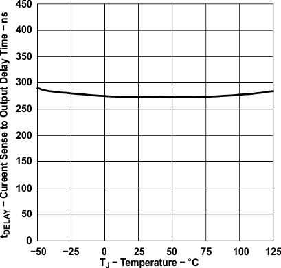
| Delay to output | CS to DRV | 300 | 450 | ns | |||
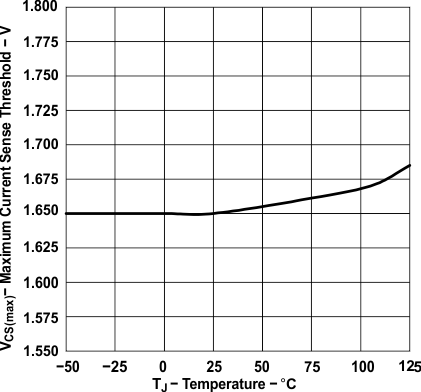
| Maximum current sense threshold voltage | 1.55 | 1.7 | 1.8 | V | |||
| PFC GATE DRIVER | |||||||
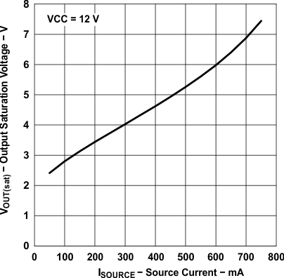
| GT1 pull-up resistance | IOUT = –125 mA | 5 | 12 | Ω | |||
| GT1 pull-down resistance | IOUT = 125 mA | 2 | 10 | Ω | |||
| GT1 output rise time | CLOAD = 1 nF, RLOAD = 10 Ω | 25 | 75 | ns | |||
| GT1 output fall time | CLOAD = 1 nF, RLOAD = 10 Ω | 10 | 50 | ns | |||
(1) Ensured by design. Not production tested.
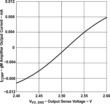
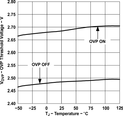
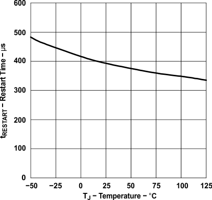
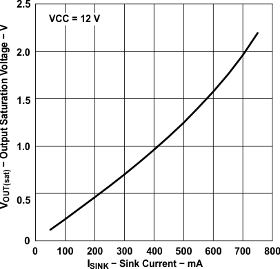
6.6 Typical Characteristics
