SLUS794F November 2007 – April 2016 UCC28070
PRODUCTION DATA.
- 1 Features
- 2 Applications
- 3 Description
- 4 Revision History
- 5 Pin Configuration and Functions
- 6 Specifications
-
7 Detailed Description
- 7.1 Overview
- 7.2 Functional Block Diagram
- 7.3
Feature Description
- 7.3.1 Interleaving
- 7.3.2 Programming the PWM Frequency and Maximum Duty-Cycle Clamp
- 7.3.3 Frequency Dithering (Magnitude and Rate)
- 7.3.4 External Clock Synchronization
- 7.3.5 Multi-phase Operation
- 7.3.6 VSENSE and VINAC Resistor Configuration
- 7.3.7 VSENSE and VINAC Open-Circuit Protection
- 7.3.8 Current Synthesizer
- 7.3.9 Programmable Peak Current Limit
- 7.3.10 Linear Multiplier and Quantized Voltage Feed Forward
- 7.3.11 Enhanced Transient Response (VA Slew-Rate Correction)
- 7.3.12 Voltage Biasing (VCC and VVREF)
- 7.3.13 PFC Enable and Disable
- 7.3.14 Adaptive Soft Start
- 7.3.15 PFC Start-Up Hold Off
- 7.3.16 Output Overvoltage Protection (OVP)
- 7.3.17 Zero-Power Detection
- 7.3.18 Thermal Shutdown
- 7.3.19 Current Loop Compensation
- 7.3.20 Voltage Loop Compensation
- 7.4 Device Functional Modes
-
8 Application and Implementation
- 8.1 Application Information
- 8.2
Typical Application
- 8.2.1 Design Requirements
- 8.2.2
Detailed Design Procedure
- 8.2.2.1 Output Current Calculation
- 8.2.2.2 Bridge Rectifier
- 8.2.2.3 PFC Inductor (L1 and L2)
- 8.2.2.4 PFC MOSFETs (M1 and M2)
- 8.2.2.5 PFC Diode
- 8.2.2.6 PFC Output Capacitor
- 8.2.2.7 Current Loop Feedback Configuration (Sizing of the Current Transformer Turns Ratio and Sense Resistor (RS)
- 8.2.2.8 Current Sense Offset and PWM Ramp for Improved Noise Immunity
- 8.2.3 Application Curves
- 9 Power Supply Recommendations
- 10Layout
- 11Device and Documentation Support
- 12Mechanical, Packaging, and Orderable Information
7 Detailed Description
7.1 Overview
The UCC28070 power factor corrector IC controls two CCM (Continuous Conduction Mode) Boost PFC power stages operating 180° out of phase with each other. This interleaving action reduces the input and output ripple currents so that less EMI filtering is needed and allows operation at higher power levels than a non-interleaved solution.
The UCC28070 can operate over a wide range of frequencies, making it suitable for use with both MOSFET and IGBT power switches. Multiple UCC28070 controllers can be synchronized for use in higher power applications where more than two interleaved power stages are needed.
This device is especially suited to high-performance, high-power PFC applications where the use of Average Current Mode PWM control gives low THD.
7.2 Functional Block Diagram
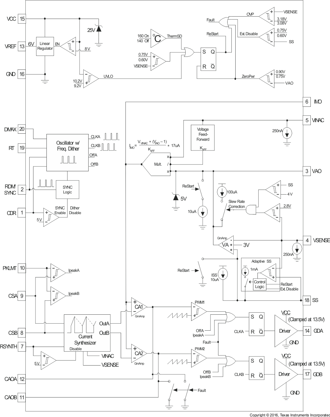
7.3 Feature Description
7.3.1 Interleaving
One of the main benefits from the 180° interleaving of phases is significant reductions in the high-frequency ripple components of both the input current and the current into the output capacitor of the PFC preregulator. Compared to that of a single-phase PFC stage of equal power, the reduced ripple on the input current eases the burden of filtering conducted-EMI noise and helps reduce the EMI filter and CIN sizes. Additionally, reduced high-frequency ripple current into the PFC output capacitor, COUT, helps to reduce its size and cost. Furthermore, with reduced ripple and average current in each phase, the boost inductor size can be smaller than in a single-phase design [1].
Ripple current reduction due to interleaving is often referred to as ripple cancellation, but strictly speaking, the peak-to-peak ripple is completely cancelled only at 50% duty-cycle in a 2-phase system. At duty-cycles other than 50%, ripple reduction occurs in the form of partial cancellation due to the superposition of the individual phase currents. Nevertheless, compared to the ripple currents of an equivalent single-phase PFC preregulator, those of a 2-phase interleaved design are extraordinarily smaller [1]. Independent of ripple cancellation, the frequency of the interleaved ripple, at both the input and output, is 2 × fPWM.
On the input, 180° interleaving reduces the peak-to-peak ripple amplitude to ½ or less of the ripple amplitude of the equivalent single-phase current.
On the output, 180° interleaving reduces the rms value of the PFC-generated ripple current in the output capacitor by a factor of slightly more than √2, for PWM duty-cycles > 50%.
This can be seen in the following derivations, adapting the method by Erickson [2].
In a single-phase PFC preregulator, the total rms capacitor current contributed by the PFC stage at all duty-cycles can be shown to be approximated by:

In a dual-phase interleaved PFC preregulator, the total rms capacitor current contributed by the PFC stage for D > 50% can be shown to be approximated by:

In these equations, IO = average PFC output load current, VO = average PFC output voltage, VM = peak of the input ac-line voltage, and η = efficiency of the PFC stage at these conditions. It can be seen that the quantity under the radical for iCrms2φ is slightly smaller than ½ of that under the radical for iCrms1φ. The rms currents shown contain both the low-frequency and the high-frequency components of the PFC output current. Interleaving reduces the high-frequency component, but not the low-frequency component.
7.3.2 Programming the PWM Frequency and Maximum Duty-Cycle Clamp
The PWM frequency and maximum duty-cycle clamps for both GDx outputs of the UCC28070 are set through the selection of the resistors connected to the RT and DMAX pins, respectively. The selection of the RT resistor (RRT) directly sets the PWM frequency (fPWM).

Once RRT has been determined, the DMAX resistor (RDMX) may be derived.

where
- DMAX is the desired maximum PWM duty-cycle
7.3.3 Frequency Dithering (Magnitude and Rate)
Frequency dithering refers to modulating the switching frequency to achieve a reduction in conducted-EMI noise beyond the capability of the line filter alone. The UCC28070 implements a triangular modulation method which results in equal time spent at every point along the switching frequency range. This total range from minimum to maximum frequency is defined as the dither magnitude, and is centered around the nominal switching frequency fPWM set with RRT. For example, a dither magnitude of 20 kHz on a nominal fPWM of 100 kHz results in a frequency range of 100 kHz ±10 kHz. Furthermore, the programmed duty-cycle clamp set by RDMX remains constant at the programmed value across the entire range of the frequency dithering.
The rate at which fPWM traverses from one extreme to the other and back again is defined as the dither rate. For example, a dither rate of 1 kHz would linearly modulate the nominal frequency from 110 kHz to 90 kHz to 110 kHz once every millisecond. A good initial design target for dither magnitude is ±10% of fPWM. Most boost components can tolerate such a spread in fPWM. The designer can then iterate around there to find the best compromise between EMI reduction, component tolerances, and loop stability.
The desired dither magnitude is set by a resistor from the RDM pin to GND, of value calculated with Equation 5:

Once the value of RRDM is determined, the desired dither rate may be set by a capacitor from the CDR pin to GND, of value calculated with Equation 6:

Frequency dithering may be fully disabled by forcing the CDR pin > 5 V or by connecting it to VREF (6 V) and connecting the RDM pin directly to GND. (If populated, the relatively high impedance of the RDM resistor may allow system switching noise to couple in and interfere with the controller timing functions if not bypassed with a low impedance path when dithering is disabled.)
If an external frequency source is used to synchronize fPWM and frequency dithering is desired, the external frequency source must provide the dither magnitude and rate functions as the internal dither circuitry is disabled to prevent undesired performance during synchronization. (See External Clock Synchronization for more details.)
7.3.4 External Clock Synchronization
The UCC28070 has also been designed to be easily synchronized to almost any external frequency source. By disabling frequency dithering (pulling CDR > 5 V), the SYNC circuitry is enabled permitting the internal oscillator to be synchronized with pulses presented on the RDM pin. To ensure a precise 180° phase shift is maintained between the GDA and GDB outputs, the frequency (fSYNC) of the pulses presented at the RDM pin must be at twice the desired fPWM. For example, if a 100-kHz switching frequency is desired, the fSYNC should be 200 kHz.

To ensure the internal oscillator does not interfere with the SYNC function, RRT must be sized to set the internal oscillator frequency at least 10% below fSYNC.

It must be noted that the PWM modulator gain is reduced by a factor equivalent to the scaled RRT due to a direct correlation between the PWM ramp current and RRT. Adjustments to the current loop gains should be made accordingly.
It must also be noted that the maximum duty-cycle clamp programmability is affected during external synchronization. The internal timing circuitry responsible for setting the maximum duty cycle is initiated on the falling edge of the synchronization pulse. Therefore, the selection of RDMX becomes dependent on the synchronization pulse width (tSYNC).
 For use in RDMX equation immediately below.
Consequently to minimize the impact of the tSYNC it is clearly advantageous to use the smallest synchronization pulse width feasible.
NOTE
When external synchronization is used, a propagation delay of approximately 50 ns to 100 ns exists between internal timing circuits and the falling edge of the SYNC signal, which may result in reduced OFF-time at the highest of switching frequencies. Therefore, RDMX should be adjusted downward slightly by (tSYNC – 0.1 μs) / tSYNC to compensate. At lower SYNC frequencies, this delay becomes an insignificant fraction of the PWM period, and can be neglected.
7.3.5 Multi-phase Operation
External synchronization also facilitates using more than 2 phases for interleaving. Multiple UCC28070s can easily be paralleled to add an even number of additional phases for higher-power applications. With appropriate phase-shifting of the synchronization signals, even more input and output ripple current cancellation can be obtained. (An odd number of phases can be accommodated if desired, but the ripple cancellation would not be optimal.) For 4-, 6-, or any 2 × n-phases (where n = the number of UCC28070 controllers), each controller should receive a SYNC signal which is 360/n degrees out of phase with each other. For a 4-phase application interleaving with two controllers, SYNC1 should be 180° out of phase with SYNC2 for optimal ripple cancellation. Similarly for a 6-phase system, SYNC1, SYNC2, and SYNC3 should be 120° out of phase with each other for optimal ripple cancellation.
In a multi-phase interleaved system, each current loop is independent and treated separately; however, there is only one common voltage loop. To maintain a single control loop, all VSENSE, VINAC, SS, IMO, and VAO signals are paralleled, respectively between the n controllers. Where current-source outputs are combined (SS, IMO, VAO), the calculated load impedances must be adjusted by 1/n to maintain the same performance as with a single controller.
Figure 18 illustrates the paralleling of two controllers for a 4-phase 90-degree-interleaved PFC system.
7.3.6 VSENSE and VINAC Resistor Configuration
The primary purpose of the VSENSE input is to provide the voltage feedback from the output to the voltage control loop. Thus, a traditional resistor-divider network must be sized and connected between the output capacitor and the VSENSE pin to set the desired output voltage based on the 3-V regulation voltage on VSENSE.
A unique aspect of the UCC28070 is the need to place the same resistor-divider network on the VIN side of the inductor to the VINAC pin. This provides the scaled input voltage monitoring needed for the linear multiplier and current synthesizer circuitry. It is not required that the actual resistance of the VINAC network be identical to the VSENSE network, but it is necessary that the attenuation (kR) of the two divider networks be equivalent for proper PFC operation.

In noisy environments, it may be beneficial for small filter capacitors to be applied to the VSENSE and VINAC inputs to avoid the destabilizing effects of excessive noise on these inputs. If applied, the RC time-constant should not exceed 100 μs on the VSENSE input to avoid significant delay in the output transient response. The RC time-constant should also not exceed 100 μs on the VINAC input to avoid degrading of the wave-shape zero-crossings. Usually, a time constant of 3 / fPWM is adequate to filter out typical noise on VSENSE and VINAC. Some design and test iteration may be required to find the optimal amount of filtering required in a particular application.
7.3.7 VSENSE and VINAC Open-Circuit Protection
Both the VSENSE and VINAC pins have been designed with an internal 250-nA current sink to ensure that in the event of an open circuit at either pin, the voltage is not left undefined, and the UCC28070 remains in a safe operating mode.
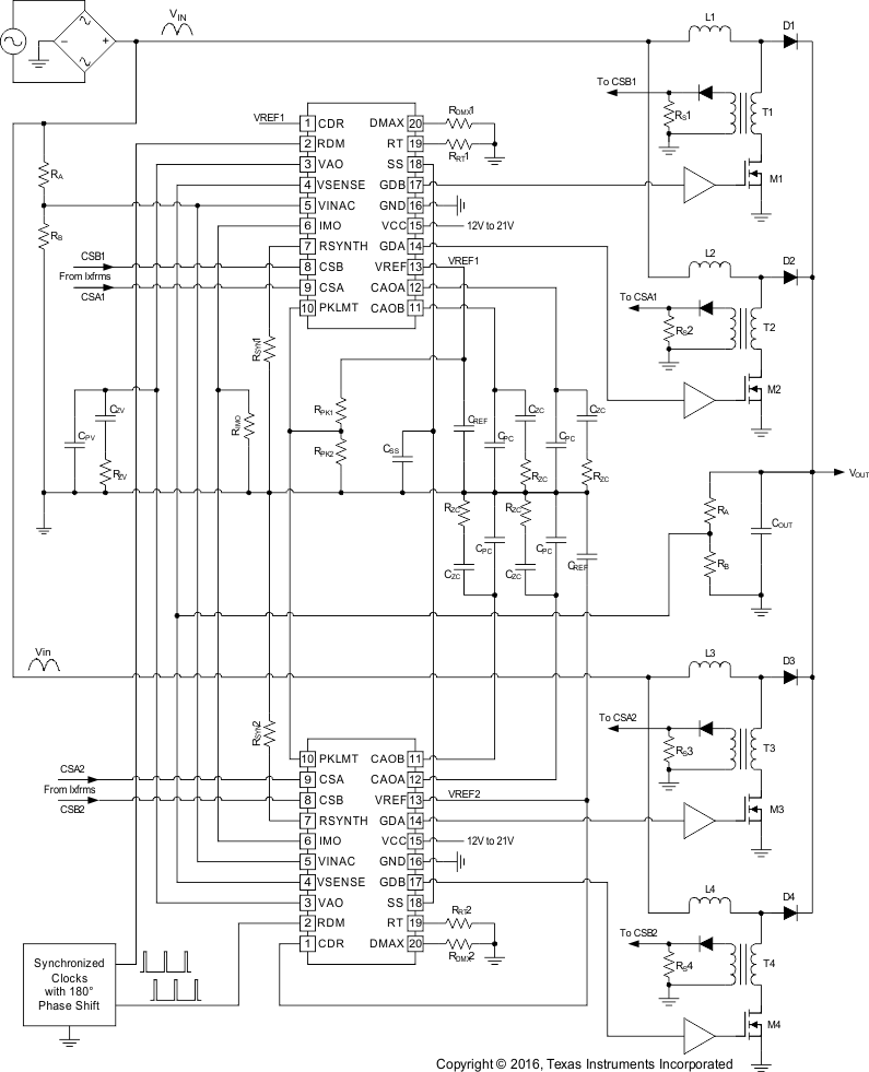 Figure 18. Simplified Four-Phase Application Diagram Using Two UCC28070 Devices
7.3.8 Current Synthesizer
One of the most prominent innovations in the UCC28070 design is the current synthesizer circuitry that synchronously monitors the instantaneous inductor current through a combination of ON-time sampling and OFF-time down-slope emulation.
During the ON-time of the GDA and GDB outputs, the inductor current is recorded at the CSA and CSB pins, respectively, through the current transformer network in each output phase. Meanwhile, the continuous monitoring of the input and output voltages through the VINAC and VSENSE pins permits the UCC28070 to internally recreate the down-slope of the inductor current during the respective OFF-time of each output. Through the selection of the RSYNTH resistor (RSYN), based on Equation 12, the internal response may be adjusted to accommodate the wide range of inductances expected across the wide array of applications.
During inrush surge events at power up and AC drop-out recovery, VVSENSE < VVINAC, the synthesized downslope becomes zero. In this case, the synthesized inductor current remains above the IMO reference and the current loop drives the duty cycle to zero. This avoids excessive stress on the MOSFETs during the surge event. Once VVINAC falls below VVSENSE, the duty cycle increases until steady-state operation resumes.
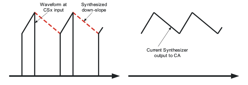 Figure 19. Downslope of the Inductor Current

where
- LB = Nominal Zero-Bias Boost Inductance (μH)
- RS = Sense Resistor (Ω)
- NCT = Current-sense Transformer turns ratio
- kR = RB / (RA + RB) = the resistor-divider attenuation at the VSENSE and VINAC pins
7.3.9 Programmable Peak Current Limit
The UCC28070 has been designed with a programmable cycle-by-cycle peak current limit dedicated to disabling either the GDA or GDB output whenever the corresponding current-sense input (CSA or CSB, respectively) rises above the voltage established on the PKLMT pin. Once an output has been disabled through the detection of peak current limit, the output remains disabled until the next clock cycle initiates a new PWM period. The programming range of the PKLMT voltage extends to upwards of 4 V to permit the full use of the 3-V average current sense signal range; however, note that the linearity of the current amplifiers begins to compress above 3.6 V.
A resistor-divider network from VREF to GND can easily program the peak current limit voltage on PKLMT, provided the total current out of VREF is less than 2 mA to avoid drooping of the 6-V VREF voltage. TI recommends a load of less than 0.5 mA, but if the resistance on PKLMT is very high, TI recommends a small filter capacitor on PKLMT to avoid operational problems in high-noise environments.
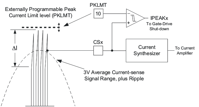 Figure 20. Externally Programmable Peak Current Limit
7.3.10 Linear Multiplier and Quantized Voltage Feed Forward
The UCC28070 multiplier generates a reference current which represents the desired wave shape and proportional amplitude of the AC input current. This current is converted to a reference voltage signal by the RIMO resistor which is scaled in value to match the voltage of the current-sense signals. The instantaneous multiplier current is dependent upon the rectified, scaled input voltage VVINAC and the voltage-error amplifier output VVAO. VVINAC conveys three pieces of information to the multiplier:
- The overall wave-shape of the input voltage (typically sinusoidal)
- The instantaneous input voltage magnitude at any point in the line cycle
- The rms level of the input voltage.
A major innovation in the UCC28070 multiplier architecture is the internal quantized VRMS feed-forward (QVFF) circuitry, which eliminates the requirement for external filtering of the VINAC signal and the subsequent slow response to transient line variations. A unique circuit algorithm detects the transition of the peak of VVINAC through seven thresholds and generates an equivalent VFF level centered within the 8-QVFF ranges. The boundaries of the ranges expand with increasing VIN to maintain an approximately equal-percentage delta between levels. These 8-QVFF levels are spaced to accommodate the full universal line range of 85 to 265 VRMS.
A great benefit of the QVFF architecture is that the fixed kVFF factors eliminate any contribution to distortion of the multiplier output, unlike an externally-filtered VINAC signal which unavoidably contains 2nd-harmonic distortion components. Furthermore, the QVFF algorithm allows for rapid response to both increasing and decreasing changes in input rms voltage so that disturbances transmitted to the PFC output are minimized. 5% hysteresis in the level thresholds help avoid chattering between QVFF levels for VVINAC voltage peaks near a particular threshold or containing mild ringing or distortion. The QVFF architecture requires that the input voltage be largely sinusoidal, and relies on detecting zero-crossings to adjust QVFF downward on decreasing input voltage. Zero-crossings are defined as VVINAC falling below 0.7 V for at least 50 μs, typically.
Table 1 shows the relationship between the various VVINAC peak voltages and the corresponding kVFF terms for the multiplier equation.
Table 1. VVINAC Peak Voltages
| LEVEL | VVINAC PEAK VOLTAGE | kVFF (V2) | VIN PEAK VOLTAGE (1) |
|---|---|---|---|
| 8 | 2.6 V ≤ VVINAC(pk) | 3.857 | >345 V |
| 7 | 2.25 V ≤ VVINAC(pk) < 2.6 V | 2.922 | 300 V to 345 V |
| 6 | 1.95 V ≤ VVINAC(pk) < 2.25 V | 2.199 | 260 V to 300 V |
| 5 | 1.65 V ≤ VVINAC(pk) < 1.95 V | 1.604 | 220 V to 260 V |
| 4 | 1.4 V ≤ VVINAC(pk) < 1.65 V | 1.156 | 187 V to 220 V |
| 3 | 1.2 V ≤ VVINAC(pk) < 1.4 V | 0.839 | 160 V to 187 V |
| 2 | 1 V ≤ VVINAC(pk) < 1.2 V | 0.600 | 133 V to 160 V |
| 1 | VVINAC(pk) ≤ 1 V | 0.398 | <133 V |
The multiplier output current IIMO for any line and load condition can thus be determined using Equation 13:

Because the kVFF value represents the scaled (VRMS)2 at the center of a level, VVAO adjusts slightly upwards or downwards when VVINAC(pk) is either lower or higher than the center of the QVFF voltage range to compensate for the difference. This is automatically accomplished by the voltage loop control when VIN varies, both within a level and after a transition between levels.
The output of the voltage-error amplifier (VVAO) is clamped at 5 V, which represents the maximum PFC output power. This value is used to calculate the maximum reference current at the IMO pin, and sets a limit for the maximum input power allowed (and, as a consequence, limits maximum output power).
Unlike a continuous VFF situation, where maximum input power is a fixed power at any VRMS input, the discrete QVFF levels permit a variation in maximum input power within limited boundaries as the input VRMS varies within each level.
The lowest maximum power limit occurs at the VVINAC voltage of 0.76 V, while the highest maximum power limit occurs at the increasing threshold from level-1 to level-2. This pattern repeats at every level transition threshold, considering that decreasing thresholds are 95% of the increasing threshold values. Below VVINAC = 0.76 V, PIN is always less than PIN(max), falling linearly to zero with decreasing input voltage.
For example, to design for the lowest maximum power allowable, determine the maximum steady-state (average) output power required of the PFC preregulator and add some additional percentage to account for line drop-out recovery power (to recharge COUT while full load power is drawn) such as 10% or 20% of POUT(max). Then apply the expected efficiency factor to find the lowest maximum input power allowable:

At the PIN(max) design threshold, VVINAC = 0.76 V, hence QVFF = 0.398 and input VAC = 73 VRMS (accounting for 2‑V bridge-rectifier drop) for a nominal 400-V output system.


This IIN(pk) value represents the combined average current through the boost inductors at the peak of the line voltage. Each inductor current is detected and scaled by a current-sense transformer (CT). Assuming equal currents through each interleaved phase, the signal voltage at each current sense input pin (CSA and CSB) is developed across a sense resistor selected to generate approximately 3 V based on ½IIN(pk) × RS / NCT, where RS is the current sense resistor and NCT is the CT turns-ratio.
IIMO is then calculated at that same lowest maximum-power point, as:

RIMO is selected such that:

Therefore:

At the increasing side of the level-1 to level-2 threshold, note that the IMO current would allow higher input currents at low-line:

However, this current may easily be limited by the programmable peak current limiting (PKLMT) feature of the UCC28070 if required by the power stage design.
The same procedure can be used to find the lowest and highest input power limits at each of the QVFF level transition thresholds. At higher line voltages, where the average current with inductor ripple is traditionally below the PKLMT threshold, the full variation of maximum input power is seen, but the input currents are inherently below the maximum acceptable current levels of the power stage.
The performance of the multiplier in the UCC28070 has been significantly enhanced when compared to previous generation PFC controllers, with high linearity and accuracy over most of the input ranges. The accuracy is at its worst as VVAO approaches 1 V because the error of the (VVAO – 1) subtraction increases and begins to distort the IMO reference current to a greater degree.
7.3.11 Enhanced Transient Response (VA Slew-Rate Correction)
Due to the low-voltage loop bandwidth required to maintain proper PFC and ignore the slight ripple at twice line frequency on the output, the response of ordinary controllers to input voltage and load transients are also slow. However, the QVFF function effectively handles the line transient response with the exception of any minor adjustments needed within a QVFF level. Load transients on the other hand can only be handled by the voltage loop; therefore, the UCC28070 has been designed to improve its transient response by pulling up on the output of the voltage amplifier (VVAO) with an additional 100 μA of current in the event the voltage on VSENSE drops below 93% of regulation (2.79 V). During a soft-start cycle, when VVSENSE is ramping up from the 0.75-V PFC Enable threshold, the 100-μA correction current source is disabled to ensure the gradual and controlled ramping of output voltage and current during a soft start.
7.3.12 Voltage Biasing (VCC and VVREF)
The UCC28070 operates within a VCC bias supply range of 10 V to 21 V. An undervoltage lockout (UVLO) threshold prevents the PFC from activating until VCC > 10.2 V, and 1 V of hysteresis assures reliable start-up from a possibly low-compliance bias source. An internal 25-V Zener-like clamp on the VCC pin is intended only to protect the device from brief energy-limited surges from the bias supply, and should not be used as a regulator with a current-limited source.
At minimum, a 0.1-μF ceramic bypass capacitor must be applied from VCC to GND close to the device pins to provide local filtering of the bias supply. Larger values may be required depending on ICC peak current magnitudes and durations to minimize ripple voltage on VCC.
To provide a smooth transition out of UVLO and to make the 6-V voltage reference available as early as possible, the output from VREF is enabled when VCC exceeds 8 V typically.
The VREF circuitry is designed to provide the biasing of all internal control circuits and for limited use externally. At minimum, a 22-nF ceramic bypass capacitor must be applied from VREF to GND close to the device pins to ensure stability of the circuit. External load current on the VREF pin should be limited to less than 2 mA, or degraded regulation may result.
7.3.13 PFC Enable and Disable
The UCC28070 contains two independent circuits dedicated to disabling the GDx outputs based on the biasing conditions of the VSENSE or SS pins. The first is a PFC Enable which monitors VVSENSE and holds off soft-start and the overall PFC function until the output has pre-charged to approximately 25%. Prior to VVSENSE reaching 0.75 V, almost all of the internal circuitry is disabled. Once VVSENSE reaches 0.75 V and VVAO < 0.75 V, the oscillator, multiplier, and current synthesizer are enabled and the SS circuitry begins to ramp up the voltage on the SS pin. The second circuit provides an external interface to emulate an internal fault condition to disable the GDx output without fully disabling the voltage loop and multiplier. By externally pulling the SS pin below 0.6 V, the GDx outputs are immediately disabled and held low. Assuming no other fault conditions are present, normal PWM operation resumes when the external SS pulldown is released. The external pulldown must be sized large enough to override the internal 1.5-mA adaptive SS pullup once the SS voltage falls below the disable threshold. TI recommends using a MOSFET with less than 100-Ω RDS(on) resistance to ensure the SS pin is held adequately below the disable threshold.
7.3.14 Adaptive Soft Start
To maintain a controlled power up, the UCC28070 has been designed with an adaptive soft-start function that overrides the internal reference voltage with a controlled voltage ramp during power up. On initial power up, once VVSENSE exceeds the 0.75-V enable threshold (VEN), the internal pulldown on the SS pin is released, and the 1.5‑mA adaptive soft-start current source is activated. This 1.5-mA pull-up almost immediately pulls the SS pin to 0.75 V (VVSENSE) to bypass the initial 25% of dead time during a traditional 0 V to Vregulation SS ramp. Once the SS pin has reached the voltage on VSENSE, the 10-μA soft-start current (ISS) takes over. Thus, through the selection of the soft-start capacitor (CSS), the effective soft-start time (tSS) may be easily programmed based on Equation 21.

Often, a system restart is desired following a brief shut-down. In such a case, VSENSE may still have substantial voltage if VOUT has not fully discharged or if high line has peak charged COUT. To eliminate the delay caused by charging CSS from 0 V up to the precharged VVSENSE with only the 10-μA current source and minimize any further output voltage sag, the adaptive soft start uses a 1.5-mA current source to rapidly charge CSS to VVSENSE, after which time the 10-μA source controls the VSS rise at the desired soft-start ramp rate. In such a case, tSS is estimated as follows:

where
- VVSENSE0 is the voltage at VSENSE at the moment a soft start or restart is initiated
NOTE
For soft start to be effective and avoid overshoot on VOUT, the SS ramp must be slower than the voltage-loop control response. Choose CSS ≥ CVZ to ensure this.
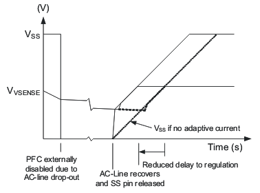 Figure 21. Soft-Start Ramp Rate
7.3.15 PFC Start-Up Hold Off
An additional feature designed into the UCC28070 is the Start-Up Hold Off logic that prevents the device from initiating a soft-start cycle until the VAO pin is below the zero-power threshold (0.75 V). This feature ensures that the SS cycle initiates from zero-power and zero duty-cycle while preventing the potential for any significant inrush currents due to stored charge in the VAO compensation network.
7.3.16 Output Overvoltage Protection (OVP)
Because of the high voltage output and a limited design margin on the output capacitor, output overvoltage protection is essential for PFC circuits. The UCC28070 implements OVP through the continuous monitoring of VVSENSE. In the event VVSENSE rises above 106% of regulation (3.18 V), the GDx outputs are immediately disabled to prevent the output voltage from reaching excessive levels. Meanwhile the CAOx outputs are pulled low to ensure a controlled recovery starting from 0% duty-cycle after an OVP fault is released. Once VVSENSE has dropped below 3.08 V, the PWM operation resumes normal operation.
7.3.17 Zero-Power Detection
To prevent undesired performance under no-load and near no-load conditions, the UCC28070 zero-power detection comparator is designed to disable both GDA and GDB outputs in the event VVAO voltage falls below 0.75 V. The 150 mV of hysteresis ensures that the outputs remain disabled until VVAO has nearly risen back into the linear range of the multiplier (VVAO ≥ 0.9 V).
7.3.18 Thermal Shutdown
To protect the power supplies from silicon failures at excessive temperatures, the UCC28070 has an internal temperature-sensing comparator that shuts down nearly all of the internal circuitry, and disables the GDA and GDB outputs, if the die temperature rises above 160°C. Once the die temperature falls below 140°C, the device brings the outputs up through a typical soft start.
7.3.19 Current Loop Compensation
The UCC28070 incorporates two identical and independent transconductance-type current-error amplifiers (one for each phase) with which to control the shaping of the PFC input current waveform. The current-error amplifier (CA) forms the heart of the embedded current control loop of the boost PFC preregulator, and is compensated for loop stability using familiar principles [4, 5]. The output of the CA for phase-A is CAOA, and that for phase-B is CAOB. Because the design considerations are the same for both, they are collectively referred to as CAOx, where x is A or B.
In a boost PFC preregulator, the current control loop comprises the boost power plant stage, the current sensing circuitry, the wave-shape reference, the PWM stage, and the CA with compensation components. The CA compares the average boost inductor current sensed with the wave-shape reference from the multiplier stage and generates an output current proportional to the difference.
This CA output current flows through the impedance of the compensation network generating an output voltage, VCAO, which is then compared with a periodic voltage ramp to generate the PWM signal necessary to achieve PFC.
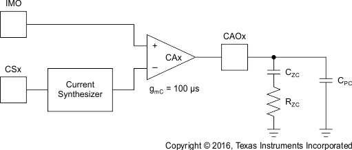 Figure 22. Current Error Amplifier With Type II Compensation
For frequencies above boost LC resonance and below fPWM, the small-signal model of the boost stage, which includes current sensing, can be simplified to:

where
- LB = mid-value boost inductance
- RS = CT sense resistor
- NCT = CT turns ratio
- VOUT = average output voltage
- ∆VRMP = 4 Vpk-pk amplitude of the PWM voltage ramp
- kSYNC = ramp reduction factor (if PWM frequency is synchronized to an external oscillator; kSYNC = 1, otherwise)
- s = Laplace complex variable
An RZCCZC network is introduced on CAOx to obtain high gain for the low-frequency content of the inductor current signal, but reduced flat gain above the zero frequency out to fPWM to attenuate the high-frequency switching ripple content of the signal (thus averaging it).
The switching ripple voltage should be attenuated to less than 1/10 of the ΔVRMP amplitude so as to be considered negligible ripple.
Thus, CAOx gain at fPWM is:

where
- ∆ILB is the maximum peak-to-peak ripple current in the boost inductor
- gmc is the transconductance of the CA, 100 μS

The current-loop cross-over frequency is then found by equating the open loop gain to 1 and solving for fCXO:

CCZ is then determined by setting fZC = fCXO = 1 / (2πRZC × CZC) and solving for CZC. At fZC = fCXO, a phase margin of 45° is obtained at fCXO. Greater phase margin may be had by placing fZC < fCXO.
An additional high-frequency pole is generally added at fPWM to further attenuate ripple and noise at fPWM and higher. This is done by adding a small-value capacitor, Cpc, across the RzcCzcnetwork.

The procedure above is valid for fixed-value inductors.
NOTE
If a swinging-choke boost inductor (inductance decreases with increasing current) is used, fCXO varies with inductance, so CZC should be determined at maximum inductance.
7.3.20 Voltage Loop Compensation
The outer voltage control loop of the dual-phase PFC controller functions the same as with a single-phase controller, and compensation techniques for loop stability are standard [4]. The bandwidth of the voltage-loop must be considerably lower than the twice-line ripple frequency (f2LF) on the output capacitor to avoid distortion-causing correction to the output voltage. The output of the voltage-error amplifier (VVAO) is an input to the multiplier to adjust the input current amplitude relative to the required output power. Variations on VAO within the bandwidth of the current loops influences the wave-shape of the input current. Because the low-frequency ripple on COUT is a function of input power only, its peak-to-peak amplitude is the same at high-line as at low-line. Any response of the voltage-loop to this ripple has a greater distorting effect on high-line current than on low-line current. Therefore, the allowable percentage of 3rd-harmonic distortion on the input current contributed by VAO should be determined using high-line conditions.
Because the voltage-error amplifier (VA) is a transconductance type of amplifier, the impedance on its input has no bearing on the amplifier gain, which is determined solely by the product of its transconductance (gmv) with its output impedance (ZOV). Thus, the VSENSE input divider-network values are determined separately based on criteria discussed in VSENSE and VINAC Resistor Configuration. Its output is the VAO pin.
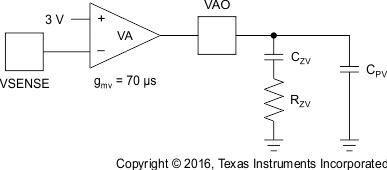 Figure 23. Voltage Error Amplifier With Type II Compensation
The twice-line ripple voltage component of VVSENSE must be sufficiently attenuated and phase-shifted at VAO to achieve the desired level of 3rd-harmonic distortion of the input current wave-shape [4]. For every 1% of 3rd-harmonic input distortion allowable, the small-signal gain GVEA = VVAOpk / vSENSEpk = gmv × ZOV at the twice-line frequency should allow no more than 2% ripple over the full VVAO voltage range. In the UCC28070, VVAO can range from 1 V at zero load power to ~4.2 V at full load power for a ΔVVAO = 3.2 V, so 2% of 3.2 V is 64-mV peak ripple.
NOTE
Although the maximum VVAO is clamped at 5 V, at full load VVAO may vary around an approximate center point of 4.2 V to compensate for the effects of the quantized feed-forward voltage in the multiplier stage (see Linear Multiplier and Quantized Voltage Feed Forward for details). Therefore, 4.2 V is the proper voltage to use to represent maximum output power when performing voltage-loop gain calculations.
The output capacitor maximum low-frequency, zero-to-peak, ripple voltage is closely approximated by:

where
- PIN(avg) is the total maximum input power of the interleaved-PFC preregulator
- VOUT(avg) is the average output voltage
- COUT is the output capacitance
where
- kR is the gain of the resistor-divider network on VSENSE
Thus, for k3rd, the percentage of allowable 3rd-harmonic distortion on the input current attributable to the VAO ripple,

This impedance on VAO is set by a capacitor (CPV), where CPV = 1 / (2πf2LF × ZOV(f2LF)); therefore:

The voltage-loop unity-gain cross-over frequency (fVXO) may now be solved by setting the open-loop gain equal to 1:


The zero-resistor (RZV) from the zero-placement network of the compensation may now be calculated. Together with CPV, RZV sets a pole right at fVXO to obtain 45° phase margin at the cross-over.

Finally, a zero is placed at or below fVXO / 6 with capacitor CZV to provide high gain at DC but with a breakpoint far enough below fVXO so as not to significantly reduce the phase margin. Choosing fVXO / 10 allows one to approximate the parallel combination value of CZV and CPV as CZV, and solve for CZV simply as:

By using a spreadsheet or math program, CZV, RZV, and CPV may be manipulated to observe their effects on fVXO and phase margin and the percentage contribution to 3rd-harmonic distortion. Also, phase margin may be checked as PIN(avg) level and system parameter tolerances vary.
NOTE
The percent of 3rd-harmonic distortion calculated in this section represents the contribution from the f2LF voltage ripple on COUT only. Other sources of distortion, such as the current-sense transformer, the current synthesizer stage, even distorted VIN, and so on, can contribute additional 3rd and higher order harmonic distortion.
7.4 Device Functional Modes
The UCC28070 operates in Average Current Mode. This eliminates the peak-to-average current error inherent in the peak current mode control method and gives lower THD and harmonics on the current drawn from the line. It does not require slope compensation and has better noise immunity than the peak current control method.