SLUS794F November 2007 – April 2016 UCC28070
PRODUCTION DATA.
- 1 Features
- 2 Applications
- 3 Description
- 4 Revision History
- 5 Pin Configuration and Functions
- 6 Specifications
-
7 Detailed Description
- 7.1 Overview
- 7.2 Functional Block Diagram
- 7.3
Feature Description
- 7.3.1 Interleaving
- 7.3.2 Programming the PWM Frequency and Maximum Duty-Cycle Clamp
- 7.3.3 Frequency Dithering (Magnitude and Rate)
- 7.3.4 External Clock Synchronization
- 7.3.5 Multi-phase Operation
- 7.3.6 VSENSE and VINAC Resistor Configuration
- 7.3.7 VSENSE and VINAC Open-Circuit Protection
- 7.3.8 Current Synthesizer
- 7.3.9 Programmable Peak Current Limit
- 7.3.10 Linear Multiplier and Quantized Voltage Feed Forward
- 7.3.11 Enhanced Transient Response (VA Slew-Rate Correction)
- 7.3.12 Voltage Biasing (VCC and VVREF)
- 7.3.13 PFC Enable and Disable
- 7.3.14 Adaptive Soft Start
- 7.3.15 PFC Start-Up Hold Off
- 7.3.16 Output Overvoltage Protection (OVP)
- 7.3.17 Zero-Power Detection
- 7.3.18 Thermal Shutdown
- 7.3.19 Current Loop Compensation
- 7.3.20 Voltage Loop Compensation
- 7.4 Device Functional Modes
-
8 Application and Implementation
- 8.1 Application Information
- 8.2
Typical Application
- 8.2.1 Design Requirements
- 8.2.2
Detailed Design Procedure
- 8.2.2.1 Output Current Calculation
- 8.2.2.2 Bridge Rectifier
- 8.2.2.3 PFC Inductor (L1 and L2)
- 8.2.2.4 PFC MOSFETs (M1 and M2)
- 8.2.2.5 PFC Diode
- 8.2.2.6 PFC Output Capacitor
- 8.2.2.7 Current Loop Feedback Configuration (Sizing of the Current Transformer Turns Ratio and Sense Resistor (RS)
- 8.2.2.8 Current Sense Offset and PWM Ramp for Improved Noise Immunity
- 8.2.3 Application Curves
- 9 Power Supply Recommendations
- 10Layout
- 11Device and Documentation Support
- 12Mechanical, Packaging, and Orderable Information
6 Specifications
6.1 Absolute Maximum Ratings
over operating free-air temperature range (unless otherwise noted) (1)| MIN | MAX | UNIT | ||
|---|---|---|---|---|
| Supply voltage | VCC | 22 | V | |
| Supply current, IVCC | 20 | mA | ||
| Gate drive current – continuous | GDA, GDB | ±0.25 | A | |
| Gate drive current – pulsed | GDA, GDB | ±0.75 | A | |
| Voltage | GDA, GDB | –0.5 | VCC + 0.3 | V |
| DMAX, RDM, RT, CDR, VINAC, VSENSE, SS, VAO, IMO, CSA, CSB, CAOA, CAOB, PKLMT, VREF | –0.5 | 7 | ||
| Current | RT, DMAX, RDM, RSYNTH | –0.5 | mA | |
| VREF, VAO, CAOA, CAOB, IMO | 10 | |||
| Lead temperature (10 seconds) | 260 | °C | ||
| Operating junction temperature, TJ | –40 | 125 | °C | |
| Storage temperature, Tstg | –65 | 150 | °C | |
(1) Stresses beyond those listed under Absolute Maximum Ratings may cause permanent damage to the device. These are stress ratings only, which do not imply functional operation of the device at these or any other conditions beyond those indicated under Recommended Operating Conditions. Exposure to absolute-maximum-rated conditions for extended periods may affect device reliability.
6.2 ESD Ratings
| VALUE | UNIT | |||
|---|---|---|---|---|
| V(ESD) | Electrostatic discharge | Human-body model (HBM), per ANSI/ESDA/JEDEC JS-001(1) | 2000 | V |
| Charged-device model (CDM), per JEDEC specification JESD22-C101(2) | 500 | |||
(1) JEDEC document JEP155 states that 500-V HBM allows safe manufacturing with a standard ESD control process.
(2) JEDEC document JEP157 states that 250-V CDM allows safe manufacturing with a standard ESD control process.
6.3 Recommended Operating Conditions
over operating free-air temperature range (unless otherwise noted)| MIN | MAX | UNIT | |||
|---|---|---|---|---|---|
| VCC | Input voltage (from a low-impedance source) | VCC | VUVLO + 1 V | 21 | V |
| Load current | VREF | 2 | mA | ||
| Input voltage range | VINAC | 0 | 3 | V | |
| Voltage range | IMO | 0 | 3.3 | V | |
| VPKLMT | Voltage range | CSA, CSB | 0 | 3.6 | V |
| RSYN | RSYNTH resistance | 15 | 750 | kΩ | |
| RRDM | RDM resistance | 30 | 330 | kΩ | |
6.4 Thermal Information
| THERMAL METRIC(1) | UCC28070 | UNIT | ||
|---|---|---|---|---|
| SOIC (DW) | TSSOP (PW) | |||
| 20 PINS | 20 PINS | |||
| RθJA | Junction-to-ambient thermal resistance | 78.1 | 99.9 | °C/W |
| RθJC(top) | Junction-to-case (top) thermal resistance | 42.5 | 34.1 | °C/W |
| RθJB | Junction-to-board thermal resistance | 46 | 50.8 | °C/W |
| ψJT | Junction-to-top characterization parameter | 17.5 | 1.9 | °C/W |
| ψJB | Junction-to-board characterization parameter | 45.5 | 50.3 | °C/W |
(1) For more information about traditional and new thermal metrics, see the Semiconductor and IC Package Thermal Metrics application report, SPRA953.
6.5 Electrical Characteristics
TA = –40°C to 125°C, TJ = TA, VCC = 12 V, GND = 0 V, RRT = 75 kΩ, RDMX = 68.1 kΩ, RRDM = RSYN = 100 kΩ, CCDR = 2.2 nF, CSS = CVREF = 0.1 μF, CVCC = 1 μF, IVREF = 0 mA (unless otherwise noted)| PARAMETER | TEST CONDITIONS | MIN | TYP | MAX | UNIT | ||
|---|---|---|---|---|---|---|---|
| BIAS SUPPLY | |||||||
| VCC(SHUNT) | VCC shunt voltage (1) | IVCC = 10 mA | 23 | 25 | 27 | V | |
| IVCC | Supply current | disabled | VVSENSE = 0 V | 7 | mA | ||
| enabled | VVSENSE = 3 V (switching) | 9 | 12 | ||||
| UVLO | VCC = 7 V | 200 | µA | ||||
| VCC = 9 V | 4 | 6 | mA | ||||
| VUVLO | UVLO turnon threshold | Measured at VCC (rising) | 9.8 | 10.2 | 10.6 | V | |
| UVLO hysteresis | Measured at VCC (falling) | 1 | |||||
| VREF enable threshold | Measured at VCC (rising) | 7.5 | 8 | 8.5 | V | ||
| LINEAR REGULATOR | |||||||
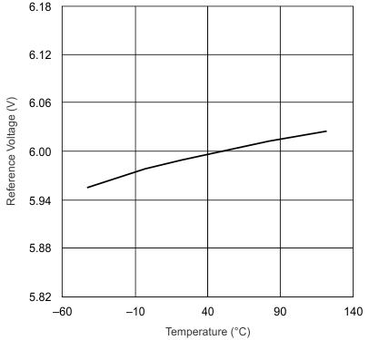
| VVREF | Reference voltage | no load | IVREF = 0 mA | 5.82 | 6 | 6.18 | V |
| load rejection | Measured as the change in VVREF
(IVREF = 0 mA and –2 mA) |
–12 | 12 | mV | |||
| line rejection | Measured as the change in VVREF
(VCC = 11 V and 20 V, IVREF = 0 μA) |
–12 | 12 | ||||
| PFC ENABLE | |||||||
| VEN | Enable threshold | Measured at VSENSE (rising) | 0.65 | 0.75 | 0.85 | V | |
| Enable hysteresis | 0.15 | ||||||
| EXTERNAL PFC DISABLE | |||||||
| Disable threshold | Measured at SS (falling) | 0.5 | 0.6 | V | |||
| Hysteresis | VVSENSE > 0.85 V | 0.15 | V | ||||
| OSCILLATOR | |||||||
| Output phase shift | Measured between GDA and GDB | 179 | 180 | 181 | ° | ||
| VDMAX, VRT, and VRDM | Timing regulation voltages | Measured at DMAX, RT, and RDM | 2.91 | 3 | 3.09 | V | |
| fPWM | PWM switching frequency | RRT = 75 kΩ, RDMX = 68.1 kΩ, VRDM = 0 V, VCDR = 6 V |
95 | 100 | 105 | kHz | |
| RRT = 24.9 kΩ, RDMX = 22.6 kΩ, VRDM = 0 V, VCDR = 6 V |
270 | 290 | 330 | ||||
| DMAX | Duty-cycle clamp | RRT = 75 kΩ, RDMX = 68.1 kΩ, VRDM = 0 V, VCDR = 6 V |
92% | 95% | 98% | ||
| Minimum programmable OFF-time | RRT = 24.9 kΩ, RDMX = 22.6 kΩ, VRDM = 0 V, VCDR = 6 V |
50 | 150 | 250 | ns | ||
| fDM | Frequency dithering magnitude change in fPWM | RRDM = 316 kΩ, RRT = 75 kΩ | 2 | 3 | 4 | kHz | |
| RRDM = 31.6 kΩ, RRT = 24.9 kΩ | 24 | 30 | 36 | ||||
| fDR | Frequency dithering rate of change in fPWM | CCDR = 2.2 nF, RRDM = 100 kΩ | 3 | kHz | |||
| CCDR = 0.3 nF, RRDM = 100 kΩ | 20 | ||||||
| ICDR | Dither rate current | Measured at CDR (sink and source) | ±10 | μA | |||
| Dither disable threshold | Measured at CDR (rising) | 5 | 5.25 | V | |||
| CLOCK SYNCHRONIZATION | |||||||
| VCDR | SYNC enable threshold | Measured at CDR (rising) | 5 | 5.25 | V | ||
| SYNC propagation delay | VCDR = 6 V, measured from RDM (rising) to GDx (rising) | 50 | 100 | ns | |||
| SYNC threshold (rising) | VCDR = 6 V, measured at RDM | 1.2 | 1.5 | V | |||
| SYNC threshold (falling) | VCDR = 6 V, measured at RDM | 0.4 | 0.7 | V | |||
| SYNC pulses | Positive pulse width | 0.2 | μs | ||||
| Maximum duty cycle (2) | 50% | ||||||
| VOLTAGE AMPLIFIER | |||||||
| VSENSE voltage | In regulation, TA = 25°C | 2.97 | 3 | 3.03 | V | ||
| VSENSE voltage | In regulation | 2.94 | 3 | 3.06 | V | ||
| VSENSE input bias current | In regulation | 250 | 500 | nA | |||
| VAO high voltage | VVSENSE = 2.9 V | 4.8 | 5 | 5.2 | V | ||
| VAO low voltage | VVSENSE = 3.1 V | 0.05 | 0.50 | V | |||
| gMV | VAO transconductance | VVSENSE = 2.8 V to 3.2 V, VVAO = 3 V | 70 | μS | |||
| VAO sink current, overdriven limit | VVSENSE = 3.5 V, VVAO = 3 V | 30 | μA | ||||
| VAO source current, overdriven | VVSENSE = 2.5 V, VVAO = 3 V, SS = 3 V | –30 | μA | ||||
| VAO source current, overdriven limit + ISRC |
VVSENSE = 2.5 V, VVAO = 3 V | –130 | μA | ||||
| Slew-rate correction threshold | Measured as VVSENSE (falling) / VVSENSE (regulation) | 92% | 93% | 95% | |||
| Slew-rate correction hysteresis | Measured at VSENSE (rising) | 3 | 9 | mV | |||
| ISRC | Slew-rate correction current | Measured at VAO, in addition to VAO source current | –100 | μA | |||
| Slew-rate correction enable threshold | Measured at SS (rising) | 4 | V | ||||
| VAO discharge current | VVSENSE = 0.5 V, VVAO = 1 V | 10 | μA | ||||
| SOFT-START | |||||||
| ISS | SS source current | VVSENSE = 0.9 V, VSS = 1 V | –10 | μA | |||
| Adaptive source current | VVSENSE = 2 V, VSS = 1 V | –1.5 | –2.5 | mA | |||
| Adaptive SS disable | Measured as VVSENSE – VSS | –30 | 0 | 30 | mV | ||
| SS sink current | VVSENSE = 0.5 V, VSS = 0.2 V | 0.5 | 0.9 | mA | |||
| OVERVOLTAGE | |||||||
| VOVP | OVP threshold | Measured as VVSENSE (rising) / VVSENSE (regulation) | 104% | 106% | 108% | ||
| OVP hysteresis | Measured at VSENSE (falling) | 100 | mV | ||||
| OVP propagation delay | Measured between VSENSE (rising) and GDx (falling) | 0.2 | 0.3 | μs | |||
| ZERO-POWER | |||||||
| VZPWR | Zero-power detect threshold | Measured at VAO (falling) | 0.65 | 0.75 | V | ||
| Zero-power hysteresis | 0.15 | V | |||||
| MULTIPLIER | |||||||
| kMULT | Gain constant | VVAO ≥ 1.5 V, TA = 25°C | 16 | 17 | 18 | μA | |
| VVAO = 1.2 V, TA = 25°C | 14.5 | 17 | 19.5 | ||||
| VVAO ≥ 1.5 V | 15 | 17 | 19 | ||||
| VVAO = 1.2 V | 13 | 17 | 21 | ||||
| IIMO | Output current: zero | VVINAC = 0.9 VPK, VVAO = 0.8 V | –0.2 | 0 | 0.2 | μA | |
| VVINAC = 0 V, VVAO = 5 V | –0.2 | 0 | 0.2 | ||||
| QUANTIZED VOLTAGE FEED-FORWARD | |||||||
| VLVL1 | Level 1 threshold (3) | Measured at VINAC (rising) | 0.6 | 0.7 | 0.8 | V | |
| VLVL2 | Level 2 threshold | 1 | V | ||||
| VLVL3 | Level 3 threshold | 1.2 | V | ||||
| VLVL4 | Level 4 threshold | 1.4 | V | ||||
| VLVL5 | Level 5 threshold | 1.65 | V | ||||
| VLVL6 | Level 6 threshold | 1.95 | V | ||||
| VLVL7 | Level 7 threshold | 2.25 | V | ||||
| VLVL8 | Level 8 threshold | 2.6 | V | ||||
| CURRENT AMPLIFIERS | |||||||
| CAOx high voltage | 5.75 | 6 | V | ||||
| CAOx low voltage | 0.1 | V | |||||
| gMC | CAOx transconductance | 100 | μS | ||||
| CAOx sink current, overdriven | 50 | μA | |||||
| CAOx source current, overdriven | –50 | μA | |||||
| Input common mode range | 0 | 3.6 | V | ||||
| Input offset voltage | VRSYNTH = 6 V, TA = 25°C | –4 | –8 | –13 | mV | ||
| VRSYNTH = 6 V | 0 | –8 | –20 | ||||
| Input offset voltage | 0 | –8 | –20 | mV | |||
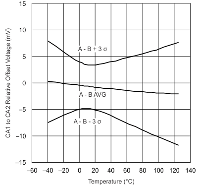
| Phase mismatch | Measured as phase A input offset minus phase B input offset | –12 | 0 | 12 | mV | ||
| CAOx pulldown current | VVSENSE = 0.5 V, VCAOx = 0.2 V | 0.5 | 0.9 | mA | |||
| CURRENT SYNTHESIZER | |||||||
| VRSYNTH | Regulation voltage | VVSENSE = 3 V, VVINAC = 0 V | 2.91 | 3 | 3.09 | V | |
| VVSENSE = 3 V, VVINAC = 2.85 V | 0.10 | 0.15 | 0.20 | ||||
| Synthesizer disable threshold | Measured at RSYNTH (rising) | 5 | 5.25 | V | |||
| VINAC input bias current | 0.250 | 0.500 | μA | ||||
| PEAK CURRENT LIMIT | |||||||
| Peak current limit threshold | VPKLMT = 3.30 V, measured at CSx (rising) | 3.27 | 3.3 | 3.33 | V | ||
| Peak current limit propagation delay | Measured between CSx (rising) and GDx (falling) edges | 60 | 100 | ns | |||
| PWM RAMP | |||||||
| VRMP | PWM ramp amplitude | 3.8 | 4 | 4.2 | V | ||
| PWM ramp offset voltage | TA = 25°C, RRT = 75 kΩ | 0.65 | 0.7 | V | |||
| PWM ramp offset temperature coefficient | –2 | mV/°C | |||||
| GATE DRIVE | |||||||
| GDA, GDB output voltage, high, clamped | VCC = 20 V, CLOAD = 1 nF | 11.5 | 13 | 15 | V | ||
| GDA, GDB output voltage, high | CLOAD = 1 nF | 10 | 10.5 | V | |||
| GDA, GDB output voltage, low | CLOAD = 1 nF | 0.2 | 0.3 | V | |||
| Rise time GDx | 1 V to 9 V, CLOAD = 1 nF | 18 | 30 | ns | |||
| Fall time GDx | 9 V to 1 V, CLOAD = 1 nF | 12 | 25 | ns | |||
| GDA, GDB output voltage, UVLO | VCC = 0 V, IGDA, IGDB = 2.5 mA | 0.7 | 2 | V | |||
(1) Excessive VCC input voltage or current damages the device. This clamp does not protect the device from an unregulated supply. If an unregulated supply is used, TI recommends a series-connected fixed positive voltage regulator such as a UA78L15A. See Absolute Maximum Ratings for the limits on VCC voltage and current.
(2) Due to the influence of the synchronization pulse width on the programmability of the maximum PWM switching duty cycle (DMAX), TI recommends minimizing the synchronization signal duty cycle.
(3) The Level 1 threshold represents the zero-crossing detection threshold above which VVINAC must rise to initiate a new input half-cycle, and below which VVINAC must fall to terminate that half-cycle.
6.6 Typical Characteristics
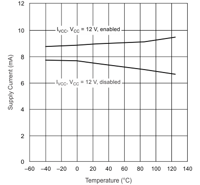
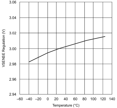 Figure 3. VVSENSE Regulation vs Junction Temperature
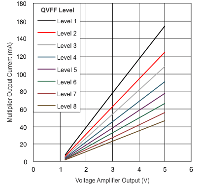 Figure 5. IMO, Multiplier Output Current vs VVAO
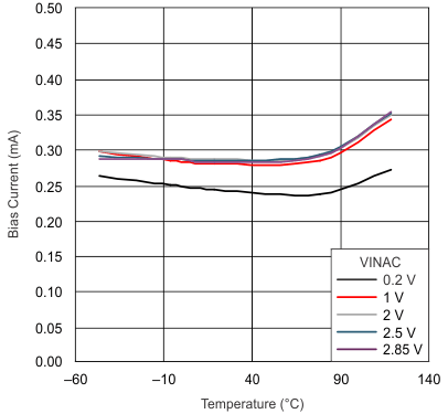 Figure 7. IVINAC Bias Current vs Junction Temperature
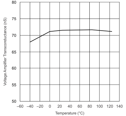 Figure 9. VAO, Voltage Amplifier Transconductance vs Junction Temperature
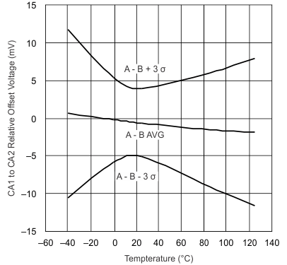
| 0.8-V Common Mode | ||
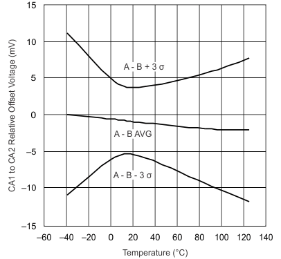
| 2-V Common Mode |
| 3.6-V Common Mode |
| VVREF = 0 mA |
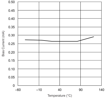 Figure 4. IVSENSE Bias Current vs Junction Temperature
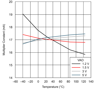 Figure 6. Multiplier Constant vs Junction Temperature
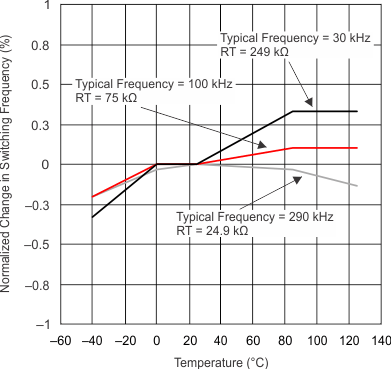 Figure 8. Normalized Switching Frequency vs Junction Temperature
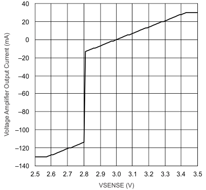 Figure 10. Voltage Amplifier Transfer Function vs VVSENSE
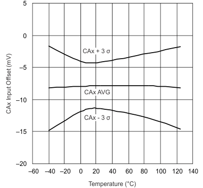
| 0.8-V Common Mode | ||
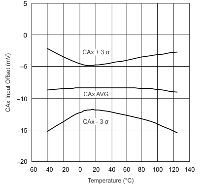
| 2-V Common Mode |
| 3.6-V Common Mode | ||