SLUS828D December 2008 – October 2017 UCC28019A
PRODUCTION DATA.
- 1 Features
- 2 Applications
- 3 Description
- 4 Revision History
- 5 Pin Configuration and Functions
- 6 Specifications
-
7 Detailed Description
- 7.1 Overview
- 7.2 Functional Block Diagram
- 7.3
Feature Description
- 7.3.1 Soft-Start
- 7.3.2
System Protection
- 7.3.2.1 VCC Undervoltage Lockout (UVLO)
- 7.3.2.2 Input Brown-Out Protection (IBOP)
- 7.3.2.3 Output Overvoltage Protection (OVP)
- 7.3.2.4 Open Loop Protection/Standby (OLP/Standby)
- 7.3.2.5 ISENSE Open-Pin Protection (ISOP)
- 7.3.2.6 Output Undervoltage Detection (UVD) and Enhanced Dynamic Response (EDR)
- 7.3.2.7 Over-Current Protection
- 7.3.2.8 Soft Over Current (SOC)
- 7.3.2.9 Peak Current Limit (PCL)
- 7.3.2.10 Current Sense Resistor, RISENSE
- 7.3.3 Gate Driver
- 7.3.4 Current Loop
- 7.3.5 ISENSE and ICOMP Functions
- 7.3.6 Pulse Width Modulator
- 7.3.7 Control Logic
- 7.3.8 Voltage Loop
- 7.3.9 Output Sensing
- 7.3.10 Voltage Error Amplifier
- 7.3.11 Non-Linear Gain Generation
- 7.4 Device Functional Modes
- 8 Application and Implementation
- 9 Power Supply Recommendations
- 10Layout
- 11Device and Documentation Support
- 12Mechanical, Packaging, and Orderable Information
7 Detailed Description
7.1 Overview
The UCC28019A is a switch-mode controller used in boost converters for power factor correction operating at a fixed frequency in continuous conduction mode. The UCC28019A requires few external components to operate as an active PFC pre-regulator. Its trimmed oscillator provides a nominal fixed switching frequency of 65 kHz, ensuring that both the fundamental and second harmonic components of the conducted-EMI noise spectrum are below the EN55022 conducted-band 150 kHz measurement limit.
Its tightly-trimmed internal 5-V reference voltage provides for accurate output voltage regulation over the typical world-wide 85-265VAC mains input range from zero to full output load.
Regulation is accomplished in two loops. The inner current loop shapes the average input current to match the sinusoidal input voltage under continuous inductor current conditions. Under light load conditions, depending on the boost inductor value, the inductor current may go discontinuous but still meet Class-D requirements of EN61000-3-2 despite the higher harmonics. The outer voltage loop regulates the PFC output voltage by generating a voltage on VCOMP (dependent upon the line and load conditions) which determines the internal gain parameters for maintaining a low-distortion steady-state input current wave-shape.
7.2 Functional Block Diagram
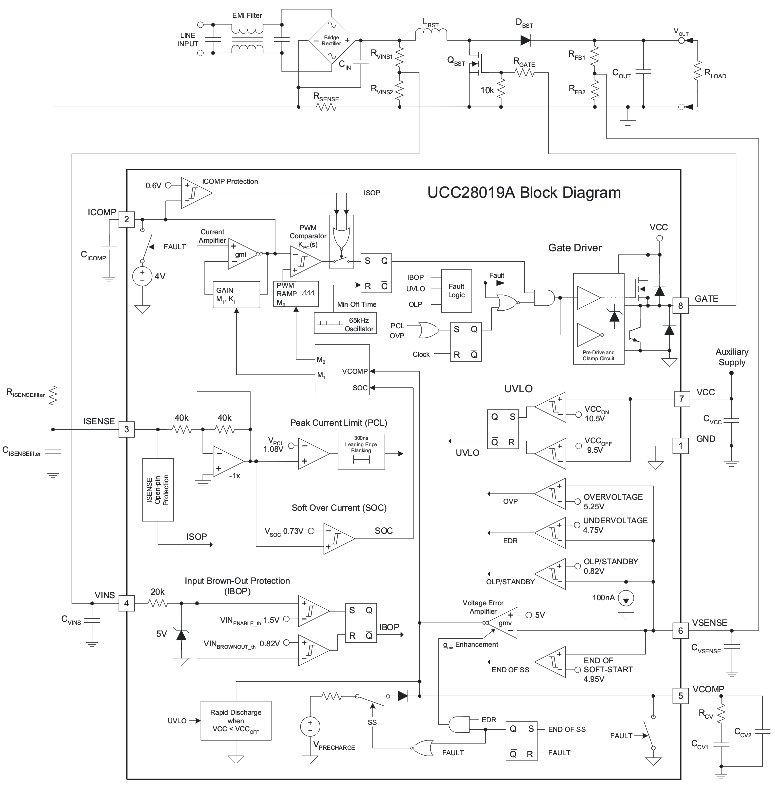
7.3 Feature Description
7.3.1 Soft-Start
Soft Start controls the rate of rise of VCOMP in order to obtain a linear control of the increasing duty cycle as a function of time. VCOMP, the output of the voltage loop transconductance amplifier, is pulled low during UVLO, IBOP, and OLP (Open-Loop Protection)/STANDBY. Once the fault condition is released, an initial pre-charge source rapidly charges VCOMP to about 1.9 V. After that point, a constant 30 μA of current is sourced into the compensation components causing the voltage on this pin to ramp linearly until the output voltage reaches 85% of its final value. At this point, the sourcing current decreases until the output voltage reaches 99% of its final rated voltage. The Soft-Start time is controlled by the voltage error amplifier compensation capacitor values selected, and is user programmable based on desired loop crossover frequency. Once the output voltage exceeds 99% of rated voltage, the pre-charge source is discountinued and EDR is no longer inhibited.
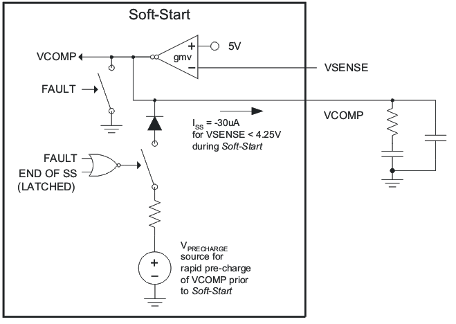 Figure 18. Soft Start
7.3.2 System Protection
System-level protection features help keep the converter within safe operating limits.
7.3.2.1 VCC Undervoltage Lockout (UVLO)
During startup, Under-Voltage Lockout (UVLO) keeps the device in the off state until VCC rises above the 10.5-V enable threshold, VCCON. With a typical 1 V of hysteresis on UVLO to increase noise immunity, the device turns off when VCC drops to the 9.5-V disable threshold, VCCOFF.
 Figure 19. UVLO
If, during a brief ac-line dropout, the VCC voltage falls below the level necessary to bias the internal FAULT circuitry, the UVLO condition enables a special rapid discharge circuit which continues to discharge the VCOMP capacitors through a low impedance despite a complete lack of VCC. This helps to avoid an excessive current surge should the ac-line return while there is still substantial voltage stored on the VCOMP capacitors. Typically, these capacitors can be discharged to less than 1.2 V within 150 ms of loss of VCC.
7.3.2.2 Input Brown-Out Protection (IBOP)
The sensed line-voltage input, VINS, provides a means for the designer to set the desired mains RMS voltage level at which the PFC pre-regulator should start-up, VACturnon, as well as the desired mains RMS level at which it should shut down, VACturnoff. This prevents unwanted sustained system operation at or below a brown-out voltage, where excessive line current could overheat components. In addition, because VCC bias is not derived directly from the line voltage, IBOP protects the circuit from low line conditions that may not trigger the VCC UVLO turn-off.
 Figure 20. Input Brown-Out Protection
Input line voltage is sensed directly from the rectified ac mains voltage through a resistor-divider filter network providing a scaled and filtered value at the VINS input. IBOP will put the device into standby mode when VINS falls (high to low) below 0.8 V, VINSBROWNOUT_th. The device comes out of standby when VINS rises (low to high) above 1.5 V, VINSENABLE_th. Bias current sourced from VINS, IVINS_0V, is less than 0.1 μA. With a bias current this low, there is little concern for any set-point error caused by this current flowing through the sensing network. The highest praticable value resistance for this network should be chosen to minimize power dissipation, especially in applications requiring low standby power. Be aware that higher resistance values are more susceptible to noise pickup, but low-noise PCB layout techniques can help mitigate this. Also, depending on the resistor type used and its voltage rating, RVINS1 should be implemented with multiple resistors in series to reduce voltage stresses.
First, select RVINS1 based on choosing the highest reasonable resistance value available for typical applications.
Then select RVINS2 based on this value:

Power dissipated in the resistor network is:

The filter capacitor, CVINS, has two functions. First, to attenuate the voltage ripple to levels between the enable and brown-out threshold to prevent ripple on VINS from falsely triggering IBOP when the converter is operating at low line. Second, CVINS delays the brown-out protection operation for a desired number of line-half-cycle periods while still having a good response to an actual brown-out event.
The capacitor is chosen so that it will discharge to the VINSBROWNOUT_th level after a delay of N number of line ½-cycles to accommodate ac-line dropout ride-through requirements.
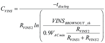
Where,

and VACmin is the lowest normal operating rms input voltage.
7.3.2.3 Output Overvoltage Protection (OVP)
VOUT(OVP) is the output voltage exceeding 5% of the rated value, causing VSENSE to exceed a 5.25-V threshold (5-V reference voltage + 5%), VOVP. The normal control loop is bypassed and the GATE output is disabled until VSENSE falls below 5.25 V. VOUT(OVP) is 420 V in a system with a 400-V rated output, for example.
7.3.2.4 Open Loop Protection/Standby (OLP/Standby)
If the output voltage feedback components were to fail and disconnect (open loop) the signal from the VSENSE input, then it is likely that the voltage error amp would increase the GATE output to maximum duty cycle. To prevent this, an internal pull-down forces VSENSE low. If the output voltage falls below 16% of its rated voltage, causing VSENSE to fall below 0.8 V, the device is put in standby, a state where the PWM switching is halted and the device is still on but draws standby current below 2.9 mA. This shutdown feature also gives the designer the option of pulling VSENSE low with an external switch.
7.3.2.5 ISENSE Open-Pin Protection (ISOP)
If the current feedback components were to fail and disconnect (open loop) the signal to the ISENSE input, then it is likely that the PWM stage would increase the GATE output to maximum duty cycle. To prevent this, an internal pull-up source drives ISENSE above 0.1 V so that a detector forces a state where the PWM switching is halted and the device is still on but draws standby current below 2.9 mA. This shutdown feature avoids continual operation in OVP and severely distorted input current.
7.3.2.6 Output Undervoltage Detection (UVD) and Enhanced Dynamic Response (EDR)
During normal operation, small perturbations on the PFC output voltage rarely exceed 5% deviation and the normal voltage control loop gain drives the output back into regulation. For large changes in line or load, if the output voltage drop exceeds -5%, an output under-voltage is detected (UVD) and Enhanced Dynamic Response (EDR) acts to speed up the slow response of the low-bandwidth voltage loop. During EDR, the transconductance of the voltage error amplifier is increased approximately 16 times to speed charging of the voltage-loop compensation capacitors to the level required for regulation. EDR is removed when VSENSE > 4.75 V. The EDR feature is not activated until soft start is completed.
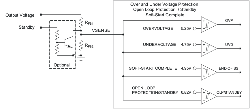 Figure 21. OVP, UVD, OLP/ Standby, Soft Start Complete
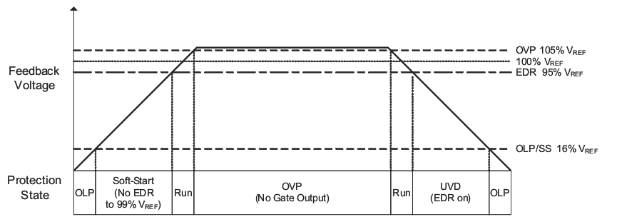 Figure 22. Soft Start and Protection States
7.3.2.7 Over-Current Protection
Inductor current is sensed by RISENSE, a low value resistor in the return path of input rectifier. The other side of the resistor is tied to the system ground. The voltage is sensed on the rectifier side of the sense resistor and is always negative. The voltage at ISENSE is buffered by a fixed gain of -1.0 to provide a positive internal signal to the current functions. There are two over-current protection features; Soft Over-Current (SOC) protects against an overload on the output and Peak Current Limit (PCL) protects against inductor saturation.
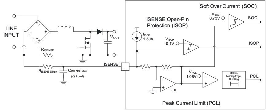 Figure 23. Soft Over Current/ Peak Current Limit
7.3.2.8 Soft Over Current (SOC)
Soft Over-Current (SOC) limits the input current. SOC is activated when the current sense voltage on ISENSE reaches -0.73 V, affecting the internal VCOMP level, and the control loop is adjusted to reduce the PWM duty cycle.
7.3.2.9 Peak Current Limit (PCL)
Peak Current Limit (PCL) operates on a cycle-by-cycle basis. When the current sense voltage on ISENSE reaches -1.08 V, PCL is activated, immediately terminating the active switch cycle. PCL is leading-edge blanked to improve noise immunity against false triggering.
7.3.2.10 Current Sense Resistor, RISENSE
The current sense resistor, RISENSE, is sized using the minimum threshold value of Soft Over Current (SOC), VSOC(min) = 0.66 V. To avoid triggering this threshold during normal operation, resulting in a decreased duty-cycle, the resistor is sized for an overload current of 10% more than the peak inductor current,

Since RISENSE sees the average input current, worst-case power dissipation occurs at input low-line when input current is at its maximum. Power dissipated by the sense resistor is given by:

Peak Current Limit (PCL) protection turns off the output driver when the voltage across the sense resistor reaches the PCL threshold, VPCL. The absolute maximum peak current, IPCL, is given by:

7.3.3 Gate Driver
The GATE output is designed with a current-optimized structure to directly drive large values of total MOSFET gate capacitance at high turn-on and turn-off speeds. An internal clamp limits voltage on the MOSFET gate to 12.5 V (typical). When VCC voltage is below the UVLO level, the GATE output is held in the Off state. An external gate drive resistor, RGATE, can be used to limit the rise and fall times and dampen ringing caused by parasitic inductances and capacitances of the gate drive circuit and to reduce EMI. The final value of the resistor depends upon the parasitic elements associated with the layout and other considerations. A 10-kΩ resistor close to the gate of the MOSFET, between the gate and ground, discharges stray gate capacitance and helps protect against inadvertent dv/dt-triggered turn-on.
 Figure 24. Gate Driver
7.3.4 Current Loop
The overall system current loop consists of the current averaging amplifier stage, the pulse width modulator (PWM) stage, the external boost inductor stage and the external current sensing resistor.
7.3.5 ISENSE and ICOMP Functions
The negative polarity signal from the current sense resistor is buffered and inverted at the ISENSE input. The internal positive signal is then averaged by the current amplifier (gmi), whose output is the ICOMP pin. The voltage on ICOMP is proportional to the average inductor current. An external capacitor to GND is applied to the ICOMP pin for current loop compensation and current ripple filtering. The gain of the averaging amplifier is determined by the internal VCOMP voltage. This gain is non-linear to accommodate the world-wide ac-line voltage range.
ICOMP is connected to 4V internally whenever the device is in a Fault or Standby condition.
7.3.6 Pulse Width Modulator
The PWM stage compares the ICOMP signal with a periodic ramp to generate a leading-edge-modulated output signal which is High whenever the ramp voltage exceeds the ICOMP voltage. The slope of the ramp is defined by a non-linear function of the internal VCOMP voltage.
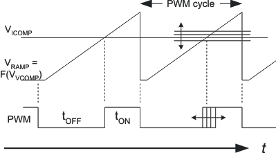 Figure 25. PWM Generation
The PWM output signal always starts Low at the beginning of the cycle, triggered by the internal clock. The output stays Low for a minimum off-time, tOFF_min, after which the ramp rises linearly to intersect the ICOMP voltage. The ramp-ICOMP intersection determines tOFF, and hence DOFF. Since DOFF = VIN/VOUT by the boost-topology equation, and since VIN is sinusoidal in wave-shape, and since ICOMP is proportional to the inductor current, it follows that the control loop forces the inductor current to follow the input voltage wave-shape to maintain boost regulation. Therefore, the average input current is also sinusoidal in wave-shape.
7.3.7 Control Logic
The output of the PWM comparator stage is conveyed to the GATE drive stage, subject to control by various protection functions incorporated into the device. The GATE output duty-cycle may be as high as 99%, but will always have a minimum off-time tOFF_min. Normal duty-cycle operation can be interrupted directly by OVP and PCL on a cycle-by-cycle basis. UVLO, IBOP and OLP/Standby also terminate the GATE output pulse, and further inhibit output until the SS operation can begin.
7.3.8 Voltage Loop
The outer control loop of the PFC controller is the voltage loop. This loop consists of the PFC output sensing stage, the voltage error amplifier stage, and the non-linear gain generation.
7.3.9 Output Sensing
A resistor-divider network from the PFC output voltage to GND forms the sensing block for the voltage control loop. The resistor ratio is determined by the desired output voltage and the internal 5-V regulation reference voltage.
Like the VINS input, the very low bias current at the VSENSE input allows the choice of the highest practicable resistor values for lowest power dissipation and standby current. A small capacitor from VSENSE to GND serves to filter the signal in a high-noise environment. This filter time constant should generally be less than 100 μs.
7.3.10 Voltage Error Amplifier
The transconductance error amplifier (gmv) generates an output current proportional to the difference between the voltage feedback signal at VSENSE and the internal 5-V reference. This output current charges or discharges the compensation network capacitors on the VCOMP pin to establish the proper VCOMP voltage for the system operating conditions. Proper selection of the compensation network components leads to a stable PFC pre-regulator over the entire ac-line range and 0-100% load range. The total capacitance also determines the rate-of-rise of the VCOMP voltage at soft start, as discussed earlier.
The amplifier output VCOMP is pulled to GND during any Fault or Standby condition to discharge the compensation capacitors to an initial zero state. Usually, the large capacitor has a series resistor which delays complete discharge for their respective time constant (which may be several hundred milliseconds). If VCC bias voltage is quickly removed after UVLO, the normal discharge transistor on VCOMP loses drive and the large capacitor could be left with substantial voltage on it, negating the benefit of a subsequent soft start. The UCC28019A incorporates a parallel discharge path which operates without VCC bias, to further discharge the compensation network after VCC is removed.
When output voltage perturbations greater than ±5% appear at the VSENSE input, the amplifier moves out of linear operation. On an over-voltage, the OVP function acts directly to shut off the GATE output until VSENSE returns within ±5% of regulation. On an under-voltage, the UVD function invokes EDR which immediately increases the voltage error amplifier transconductance to about 440 μS. This higher gain facilitates faster charging of the compensation capacitors to the new operating level.
7.3.11 Non-Linear Gain Generation
The voltage at VCOMP is used to set the current amplifier gain and the PWM ramp slope. This voltage is buffered internally and is then subject to modification by the SOC function, as discussed earlier.
Together the current gain and the PWM slope adjust to the different system operating conditions (set by the ac-line voltage and output load level) as VCOMP changes, to provide a low-distortion, high-power-factor input current wave-shape following that of the input voltage.
7.4 Device Functional Modes
This device has no functional modes.