SLUS828D December 2008 – October 2017 UCC28019A
PRODUCTION DATA.
- 1 Features
- 2 Applications
- 3 Description
- 4 Revision History
- 5 Pin Configuration and Functions
- 6 Specifications
-
7 Detailed Description
- 7.1 Overview
- 7.2 Functional Block Diagram
- 7.3
Feature Description
- 7.3.1 Soft-Start
- 7.3.2
System Protection
- 7.3.2.1 VCC Undervoltage Lockout (UVLO)
- 7.3.2.2 Input Brown-Out Protection (IBOP)
- 7.3.2.3 Output Overvoltage Protection (OVP)
- 7.3.2.4 Open Loop Protection/Standby (OLP/Standby)
- 7.3.2.5 ISENSE Open-Pin Protection (ISOP)
- 7.3.2.6 Output Undervoltage Detection (UVD) and Enhanced Dynamic Response (EDR)
- 7.3.2.7 Over-Current Protection
- 7.3.2.8 Soft Over Current (SOC)
- 7.3.2.9 Peak Current Limit (PCL)
- 7.3.2.10 Current Sense Resistor, RISENSE
- 7.3.3 Gate Driver
- 7.3.4 Current Loop
- 7.3.5 ISENSE and ICOMP Functions
- 7.3.6 Pulse Width Modulator
- 7.3.7 Control Logic
- 7.3.8 Voltage Loop
- 7.3.9 Output Sensing
- 7.3.10 Voltage Error Amplifier
- 7.3.11 Non-Linear Gain Generation
- 7.4 Device Functional Modes
- 8 Application and Implementation
- 9 Power Supply Recommendations
- 10Layout
- 11Device and Documentation Support
- 12Mechanical, Packaging, and Orderable Information
10 Layout
10.1 Layout Guidelines
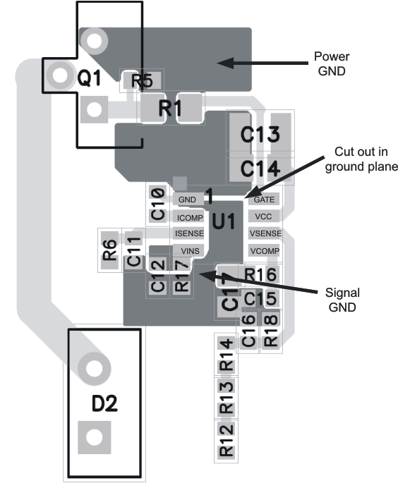
As with all PWM controllers, the effectiveness of the filter capacitors on the signal pins depends upon the integrity of the ground return. The pin out of the UCC28019A is ideally suited for separating the high di/dt induced noise on the power ground from the low current quiet signal ground required for adequate noise immunity. A star point ground connection at the GND pin of the device can be achieved with a simple cut out in the ground plane of the printed circuit board. As shown in Figure 34, the capacitors on ISENSE, VINS, VCOMP, and VSENSE must all be returned directly to the quiet portion of the ground plane, indicated by Signal GND, and not the high current return path of the converter, shown as the Power GND. Because the example circuit in Figure 34 uses surface mount components, the ICOMP capacitor, C10, has its own dedicated return to the GND pin.
Table 2. Layout Components
| REFERENCE DESIGNATOR | FUNCTION |
|---|---|
| U1 | UCC28019A |
| Q1 | Main switch |
| R1 | RGATE |
| R5 | Pull-down resistor on GATE |
| C13, C14 | VCC bypass capacitors |
| C10 | ICOMP compensation, CICOMP |
| R6 | Inrush current limiting resistor, RISENSE |
| C11 | ISENSE filter, CISENSE |
| R12, R13, R14 | RFB1 on VSENSE |
| R18 | RFB2 on VSENSE |
| C16 | CVSENSE |
| R16, C17, C15 | VCOMP compensation components, RVCOMP, CVCOMP, CVCOMP_P |
| C12, R17 | CVINS, RVINS2 on VINS |
| D2 | Boost diode |
10.2 Layout Example
 Figure 34. Recommended Layout for the UCC28019A