TPS54233 2A, 28V Input, Step Down DC/DC Converter With Eco-mode™
1 Features
- 3.5 V to 28 V Input Voltage Range
- Adjustable Output Voltage Down to 0.8 V
- Integrated 80 mΩ High Side MOSFET Supports up to 2A Continuous Output Current
- High Efficiency at Light Loads with a Pulse Skipping Eco-mode™
- Fixed 300 kHz Switching Frequency
- Typical 1 μA Shutdown Quiescent Current
- Adjustable Slow Start Limits Inrush Currents
- Programmable UVLO Threshold
- Overvoltage Transient Protection
- Cycle by Cycle Current Limit, Frequency Fold Back and Thermal Shutdown Protection
- Available in Easy-to-Use SOIC8 Package
- Supported by WEBENCH® Software Tool (www.TI.com/WEBENCH)
2 Applications
- Consumer Applications such as Set-Top Boxes, CPE Equipment, LCD Displays, Peripherals, and Battery Chargers
- Industrial and Car Audio Power Supplies
- 5V, 12V and 24V Distributed Power Systems
3 Description
The TPS54233 is a 28 V, 2 A non-synchronous buck converter that integrates a low RDS(on) high side MOSFET. To increase efficiency at light loads, a pulse skipping Eco-mode™ feature is automatically activated. Furthermore, the 1 μA shutdown supply current allows the device to be used in battery powered applications. Current mode control with internal slope compensation simplifies the external compensation calculations and reduces component count while allowing the use of ceramic output capacitors. A resistor divider programs the Hysteresis of the input under-voltage lockout. An overvoltage transient protection circuit limits voltage overshoots during startup and transient conditions. A cycle by cycle current limit scheme, frequency fold back and thermal shutdown protect the device and the load in the event of an overload condition. The TPS54233 is available in an 8-pin SOIC package that has been internally optimized to improve thermal performance.
Device Information(1)
| PART NUMBER | PACKAGE | BODY SIZE (NOM) |
|---|---|---|
| TPS54233 | SOIC (8) | 4.90 mm x 3.90 mm |
- For all available packages, see the orderable addendum at the end of the data sheet.
5 Revision History
Changes from B Revision (February 2011) to C Revision
- Added ESD Rating table, Thermal Information table, Feature Description section, Device Functional Modes, Application and Implementation section, Power Supply Recommendations section, Device and Documentation Support section, and Mechanical, Packaging sections. Go
- Deleted Features Item: For SWIFT™ Documentation, See the TI Website at www.ti.com/swiftGo
- Changed Features item: Supported by SwitcherPro™ To: Supported by WEBENCH®Go
- Changed RO1 To: R5, RO2 To R6, C1 To C6, and C2 To C7 in the Simplified SchematicGo
- Changed SwitcherPro™ Software tool To: WEBENCH Software tool in the Current Mode Compensation Design sectionGo
- Changed RO1 To: R5, RO2 To R6, C1 To C6, and C2 To C7 in the Table 1Go
- Changed the Output Voltage Set Point section. Updated the paragraph following Equation 5.Go
Changes from A Revision (March 2010) to B Revision
Changes from * Revision (October 2008) to A Revision
- Changed the Absolute Maximum Ratings table, Input Voltage - EN pin max value From: 5V to 6VGo
- Added A table to the Description - with text "For additional design needs, see.."Go
6 Pin Configuration and Functions
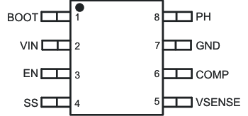
Pin Functions
| PIN | DESCRIPTION | |
|---|---|---|
| NAME | NO. | |
| BOOT | 1 | A 0.1 μF bootstrap capacitor is required between BOOT and PH. If the voltage on this capacitor falls below the minimum requirement, the high-side MOSFET is forced to switch off until the capacitor is refreshed. |
| VIN | 2 | Input supply voltage, 3.5 V to 28 V. |
| EN | 3 | Enable pin. Pull below 1.25V to disable. Float to enable. Programming the input undervoltage lockout with two resistors is recommended. |
| SS | 4 | Slow start pin. An external capacitor connected to this pin sets the output rise time. |
| VSENSE | 5 | Inverting node of the gm error amplifier. |
| COMP | 6 | Error amplifier output, and input to the PWM comparator. Connect frequency compensation components to this pin. |
| GND | 7 | Ground. |
| PH | 8 | The source of the internal high-side power MOSFET. |
7 Specifications
7.1 Absolute Maximum Ratings(1)
over operating free-air temperature range (unless otherwise noted)7.2 ESD Ratings
| VALUE | UNIT | |||
|---|---|---|---|---|
| V(ESD) | Electrostatic discharge | Human-body model (HBM), per ANSI/ESDA/JEDEC JS-001(1) | ±2000 | V |
| Charged-device model (CDM), per JEDEC specification JESD22-C101(2) | ±500 | |||
7.3 Recommended Operating Conditions
over operating free-air temperature range (unless otherwise noted)| MIN | TYP | MAX | UNIT | |
|---|---|---|---|---|
| Operating Input Voltage on (VIN pin) | 3.5 | 28 | V | |
| Operating junction temperature, TJ | –40 | 150 | °C |
7.4 Thermal Information
| THERMAL METRIC(1) | D | UNIT | |
|---|---|---|---|
| 8 PINS | |||
| RθJA | Junction-to-ambient thermal resistance | 116.7 | °C/W |
| RθJC(top) | Junction-to-case (top) thermal resistance | 62.4 | |
| RθJB | Junction-to-board thermal resistance | 57.0 | |
| ψJT | Junction-to-top characterization parameter | 14.5 | |
| ψJB | Junction-to-board characterization parameter | 56.5 | |
| RθJC(bot) | Junction-to-case (bottom) thermal resistance | N/A | |
7.5 Electrical Characteristics
TJ = –40°C to 150°C, VIN = 3.5V to 28V (unless otherwise noted)| PARAMETER | TEST CONDITIONS | MIN | TYP | MAX | UNIT |
|---|---|---|---|---|---|
| SUPPLY VOLTAGE (VIN PIN) | |||||
| Internal undervoltage lockout threshold | Rising and Falling | 3.5 | V | ||
| Shutdown supply current | EN = 0V, VIN = 12V, –40°C to 85°C | 1 | 4 | μA | |
| Operating – non switching supply current | VSENSE = 0.85 V | 75 | 110 | μA | |
| ENABLE AND UVLO (EN PIN) | |||||
| Enable threshold | Rising and Falling | 1.25 | 1.35 | V | |
| Input current | Enable threshold – 50 mV | -1 | μA | ||
| Input current | Enable threshold + 50 mV | -4 | μA | ||
| VOLTAGE REFERENCE | |||||
| Voltage reference | 0.772 | 0.8 | 0.828 | V | |
| HIGH-SIDE MOSFET | |||||
| On resistance | BOOT-PH = 3 V, VIN = 3.5 V | 115 | 200 | mΩ | |
| BOOT-PH = 6 V, VIN = 12 V | 80 | 150 | |||
| ERROR AMPLIFIER | |||||
| Error amplifier transconductance (gm) | –2 μA < I(COMP) < 2 μA, V(COMP) = 1 V | 92 | μmhos | ||
| Error amplifier DC gain(1) | VSENSE = 0.8 V | 800 | V/V | ||
| Error amplifier unity gain bandwidth(1) | 5 pF capacitance from COMP to GND pins | 2.7 | MHz | ||
| Error amplifier source/sink current | V(COMP) = 1 V, 100 mV overdrive | ±7 | μA | ||
| Switch current to COMP transconductance | VIN = 12 V | 9 | A/V | ||
| PULSE SKIPPING Eco-mode™ | |||||
| Pulse skipping Eco-mode™ switch current threshold | 100 | mA | |||
| CURRENT LIMIT | |||||
| Current limit threshold | VIN = 12 V | 2.3 | 3.5 | A | |
| THERMAL SHUTDOWN | |||||
| Thermal Shutdown | 165 | °C | |||
| SLOW START (SS PIN) | |||||
| Charge current | V(SS) = 0.4 V | 2 | μA | ||
| SS to VSENSE matching | V(SS) = 0.4 V | 10 | mV | ||
7.6 Switching Characteristics
TJ = –40°C to 150°C, VIN = 3.5 to 28 V (unless otherwise noted)| PARAMETER | TEST CONDITIONS | MIN | TYP | MAX | UNIT | |
|---|---|---|---|---|---|---|
| SWITCHING FREQUENCY | ||||||
| Device switching frequency | VIN = 12 V | 210 | 300 | 390 | kHz | |
| Minimum controllable on time | VIN = 12 V, 25°C | 105 | 130 | ns | ||
| Maximum controllable duty ratio(1) | BOOT-PH = 6 V | 90% | 93% | |||
7.7 Typical Characteristics
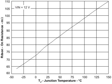 Figure 1. On Resistance vs Junction Temperature
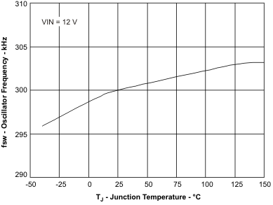 Figure 3. Switching Frequency vs Junction Temperature
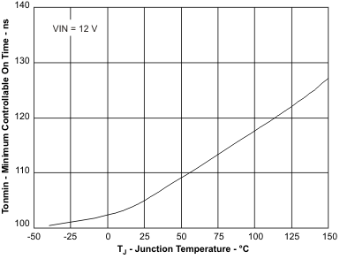 Figure 5. Minimum Controllable On Time vs
 Junction Temperature
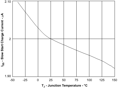 Figure 7. SS Charge Current vs Junction Temperature
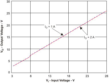 Figure 9. Typical Maximum Output Voltage vs
 Input Voltage
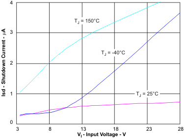 Figure 2. Shutdown Quiescent Current vs Input Voltage
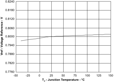 Figure 4. Voltage Reference vs Junction Temperature
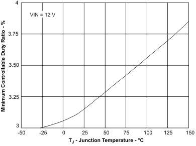 Figure 6. Minimum Controllable Duty Ratio vs
 Junction Temperature
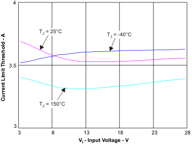 Figure 8. Current Limit Threshold vs Input Voltage
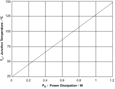 Figure 10. Maximum Power Dissipation vs
 Junction Temperature
8 Detailed Description
8.1 Overview
The TPS54233 is a 28 V, 2 A, step-down (buck) converter with an integrated high-side n-channel MOSFET. To improve performance during line and load transients, the device implements a constant frequency, current mode control which reduces output capacitance and simplifies external frequency compensation design. The TPS54233 has a pre-set switching frequency of 300 kHz.
The TPS54233 needs a minimum input voltage of 3.5 V to operate normally. The EN pin has an internal pull-up current source that can be used to adjust the input voltage under-voltage lockout (UVLO) with two external resistors. In addition, the pull-up current provides a default condition when the EN pin is floating for the device to operate. The operating current is 75 μA typically when not switching and under no load. When the device is disabled, the supply current is 1 μA typically.
The integrated 80 mΩ high-side MOSFET allows for high efficiency power supply designs with continuous output currents up to 2 A.
The TPS54233 reduces the external component count by integrating the boot recharge diode. The bias voltage for the integrated high-side MOSFET is supplied by an external capacitor on the BOOT to PH pin. The boot capacitor voltage is monitored by an UVLO circuit and will turn the high-side MOSFET off when the voltage falls below a preset threshold of 2.1 V typically. The output voltage can be stepped down to as low as the reference voltage.
By adding an external capacitor, the slow start time of the TPS54233 can be adjustable which enables flexible output filter selection.
To improve the efficiency at light load conditions, the TPS54233 enters a special pulse skipping Eco-modeTM when the peak inductor current drops below 100 mA typically.
The frequency foldback reduces the switching frequency during startup and over current conditions to help control the inductor current. The thermal shut down gives the additional protection under fault conditions.
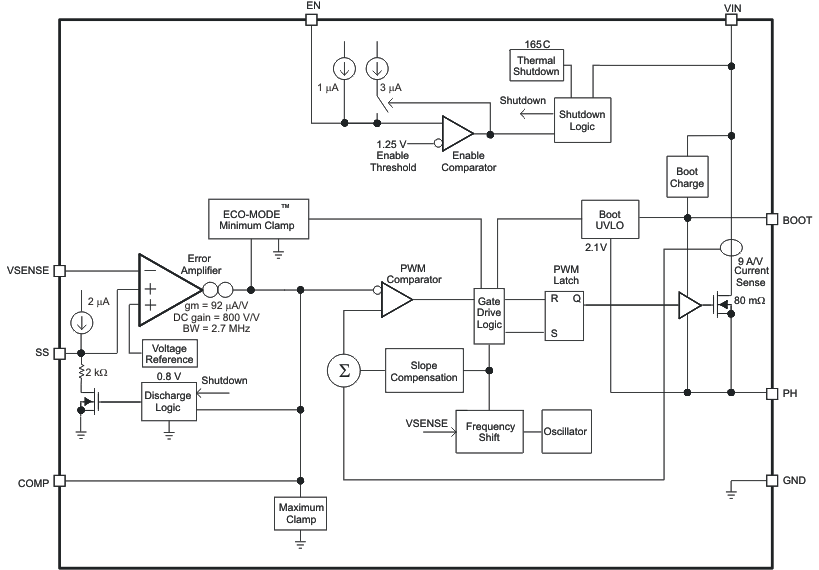
Functional Block Diagram
8.2 Feature Description
8.2.1 Fixed Frequency PWM Control
The TPS54233 uses a fixed frequency, peak current mode control. The internal switching frequency of the TPS54233 is fixed at 300kHz.
8.2.2 Voltage Reference (Vref)
The voltage reference system produces a ±2% initial accuracy voltage reference (±3.5% over temperature) by scaling the output of a temperature stable bandgap circuit. The typical voltage reference is designed at 0.8V.
8.2.3 Bootstrap Voltage (BOOT)
The TPS54233 has an integrated boot regulator and requires a 0.1 μF ceramic capacitor between the BOOT and PH pin to provide the gate drive voltage for the high-side MOSFET. A ceramic capacitor with an X7R or X5R grade dielectric is recommended because of the stable characteristics over temperature and voltage. To improve drop out, the TPS54233 is designed to operate at 100% duty cycle as long as the BOOT to PH pin voltage is greater than 2.1V typically.
8.2.4 Enable and Adjustable Input Under-Voltage Lockout (VIN UVLO)
The EN pin has an internal pull-up current source that provides the default condition of the TPS54233 operating when the EN pin floats.
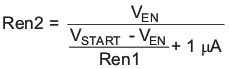
The TPS54233 is disabled when the VIN pin voltage falls below internal VIN UVLO threshold. It is recommended to use an external VIN UVLO to add Hysteresis unless VIN is greater than (VOUT + 2V). To adjust the VIN UVLO with Hysteresis, use the external circuitry connected to the EN pin as shown in Figure 11. Once the EN pin voltage exceeds 1.25V , an additional 3 μA of hysteresis is added. Use Equation 1 and Equation 2 to calculate the resistor values needed for the desired VIN UVLO threshold voltages. The VSTART is the input start threshold voltage, the VSTOP is the input stop threshold voltage and the VEN is the enable threshold voltage of 1.25 V. The VSTOP should always be greater than 3.5 V.
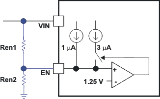 Figure 11. Adjustable Input Undervoltage Lockout

8.2.5 Programmable Slow Start Using SS PIN
It is recommended to program the slow start time externally because no slow start time is implemented internally. The TPS54233 effectively uses the lower voltage of the internal voltage reference or the SS pin voltage as the power supply’s reference voltage fed into the error amplifier and will regulate the output accordingly. A capacitor (CSS) on the SS pin to ground implements a slow start time. The TPS54233 has an internal pull-up current source of 2 μA that charges the external slow start capacitor. The equation for the slow start time (10% to 90%) is shown in Equation 3 . The Vref is 0.8 V and the ISS current is 2 μA.
The slow start time should be set between 1ms to 10ms to ensure good start-up behavior. The slow start capacitor should be no more than 27 nF.
If during normal operation, the input voltage drops below the VIN UVLO threshold, or the EN pin is pulled below 1.25 V, or a thermal shutdown event occurs, the TPS54233 stops switching.
8.2.6 Error Amplifier
The TPS54233 has a transconductance amplifier for the error amplifier. The error amplifier compares the VSENSE voltage to the internal effective voltage reference presented at the input of the error amplifier. The transconductance of the error amplifier is 92 μA/V during normal operation. Frequency compensation components are connected between the COMP pin and ground.
8.2.7 Slope Compensation
To prevent the sub-harmonic oscillations when operating the device at duty cycles greater than 50%, the TPS54233 adds a built-in slope compensation which is a compensating ramp to the switch current signal.
8.2.8 Current Mode Compensation Design
To simplify design efforts using the TPS54233, the typical designs for common applications are listed in Table 1. For designs using ceramic output capacitors, proper derating of ceramic output capacitance is recommended when doing the stability analysis. This is because the actual ceramic capacitance drops considerably from the nominal value when the applied voltage increases. See the Detailed Design Procedure section for the detailed guidelines or use the WEBENCH Software tool (www.TI.com/WEBENCH).
Table 1. Typical Designs (Refer to Section 4: Simplified Schematic
| VIN (V) |
VOUT
(V) |
Fsw
(kHz) |
LO
(μH) |
CO
|
R5 (kΩ) |
R6 (kΩ) |
C7 (pF) |
C6 (pF) |
R3 (kΩ) |
|---|---|---|---|---|---|---|---|---|---|
| 12 | 5 | 300 | 22 | Ceramic 47 μF | 10 | 1.91 | 68 | 1800 | 21 |
| 12 | 3.3 | 300 | 15 | Ceramic 47μF | 10.2 | 3.24 | 47 | 4700 | 21 |
| 12 | 1.8 | 300 | 10 | Ceramic 100 μF x 2 | 10 | 8.06 | 100 | 4700 | 21 |
| 12 | 0.9 | 300 | 6.8 | Ceramic 100 μFx2 | 10 | 80.6 | 100 | 4700 | 21 |
| 12 | 5 | 300 | 22 | Aluminum 330 μF/160 mΩ | 10 | 1.91 | 56 | 220 | 40.2 |
| 12 | 3.3 | 300 | 15 | Aluminum 470 μF/160 mΩ | 10.2 | 3.24 | 220 | 220 | 30.9 |
| 12 | 1.8 | 300 | 10 | SP 220 μF/12 mΩ | 10 | 8.06 | 100 | 4700 | 40.2 |
| 12 | 0.9 | 300 | 6.8 | SP 220 μF/12 mΩ | 10 | 80.6 | 100 | 1800 | 21 |
8.2.9 Overcurrent Protection and Frequency Shift
The TPS54233 implements current mode control that uses the COMP pin voltage to turn off the high-side MOSFET on a cycle by cycle basis. Every cycle the switch current and the COMP pin voltage are compared; when the peak inductor current intersects the COMP pin voltage, the high-side switch is turned off. During overcurrent conditions that pull the output voltage low, the error amplifier responds by driving the COMP pin high, causing the switch current to increase. The COMP pin has a maximum clamp internally, which limit the output current.
The TPS54233 provides robust protection during short circuits. There is potential for overcurrent runaway in the output inductor during a short circuit at the output. The TPS54233 solves this issue by increasing the off time during short circuit conditions by lowering the switching frequency. The switching frequency is divided by 8, 4, 2, and 1 as the voltage ramps from 0 V to 0.8 V on VSENSE pin. The relationship between the switching frequency and the VSENSE pin voltage is shown in Table 2.
Table 2. Switching Frequency Conditions
| SWITCHING FREQUENCY | VSENSE PIN VOLTAGE |
|---|---|
| 300 kHz | VSENSE ≥ 0.6 V |
| 300 kHz / 2 | 0.6 V > VSENSE ≥ 0.4 V |
| 300 kHz / 4 | 0.4 V > VSENSE ≥ 0.2 V |
| 300 kHz / 8 | 0.2 V > VSENSE |
8.2.10 Overvoltage Transient Protection
The TPS54233 incorporates an overvoltage transient protection (OVTP) circuit to minimize output voltage overshoot when recovering from output fault conditions or strong unload transients. The OVTP circuit includes an overvoltage comparator to compare the VSENSE pin voltage and internal thresholds. When the VSENSE pin voltage goes above 109% × Vref, the high-side MOSFET will be forced off. When the VSENSE pin voltage falls below 107% × Vref, the high-side MOSFET will be enabled again.
8.2.11 Thermal Shutdown
The device implements an internal thermal shutdown to protect itself if the junction temperature exceeds 165°C. The thermal shutdown forces the device to stop switching when the junction temperature exceeds the thermal trip threshold. Once the die temperature decreases below 165°C, the device reinitiates the power up sequence.
8.3 Device Functional Modes
8.3.1 Eco-modeTM
The TPS54233 is designed to operate in pulse skipping Eco-modeTM at light load currents to boost light load efficiency. When the peak inductor current is lower than 100 mA typically, the COMP pin voltage falls to 0.5V typically and the device enters Eco-mode™. When the device is in Eco-mode™, the COMP pin voltage is clamped at 0.5V internally which prevents the high side integrated MOSFET from switching. The peak inductor current must rise above 100mA for the COMP pin voltage to rise above 0.5V and exit Eco-mode™. Since the integrated current comparator catches the peak inductor current only, the average load current entering Eco-mode™ varies with the applications and external output filters.
9 Application and Implementation
NOTE
Information in the following applications sections is not part of the TI component specification, and TI does not warrant its accuracy or completeness. TI’s customers are responsible for determining suitability of components for their purposes. Customers should validate and test their design implementation to confirm system functionality.
9.1 Application Information
The TPS54233 device is typically used as a step-down converter, which converts a voltage from 3.5 V to 28 V to a lower voltage. WEBENCH software is available to aid in the design and analysis of circuits.
For additional design needs, see the following devices.
| TPS54231 | TPS54232 | TPS54233 | TPS54331 | TPS54332 | |
|---|---|---|---|---|---|
| IO(Max) | 2A | 2A | 2A | 3A | 3.5A |
| Input Voltage Range | 3.5V - 28V | 3.5V - 28V | 3.5V - 28V | 3.5V - 28V | 3.5V - 28V |
| Switching Freq. (Typ) | 570kHz | 1000kHz | 285kHz | 570kHz | 1000kHz |
| Switch Current Limit (Min) | 2.3A | 2.3A | 2.3A | 3.5A | 4.2A |
| Pin/Package | 8SOIC | 8SOIC | 8SOIC | 8SOIC | 8SO PowerPAD™ |
9.2 Typical Application
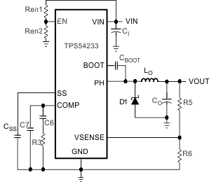
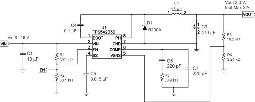 Figure 12. Typical Application Schematic
9.2.1 Design Requirements
For this design example, use the input parameters in Table 3.
Table 3. Design Parameters
| DESIGN PARAMETER | EXAMPLE VALUE |
|---|---|
| Input voltage range | 8 V to 18 V |
| Output voltage | 3.3 V |
| Input ripple voltage | 300 mV |
| Output ripple voltage | 100 mV |
| Output current rating | 2 A |
| Operating Frequency | 300 kHz |
9.2.2 Detailed Design Procedure
The following design procedure can be used to select component values for the TPS54233. Alternately, the WEBENCH Software can be used to generate a complete design. The WEBENCH Software uses an iterative design procedure and accesses a comprehensive database of components when generating a design. This section presents a simplified discussion of the design process.
9.2.2.1 Switching Frequency
The switching frequency for the TPS54233 is fixed at 300 kHz.
9.2.2.2 Output Voltage Set Point
The output voltage of the TPS54233 is externally adjustable using a resistor divider network. In the application circuit of Figure 12, this divider network is comprised of R5 and R6. The relationship of the output voltage to the resistor divider is given by Equation 4 and Equation 5:
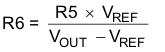
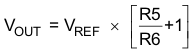
Choose R5 to be approximately 10 kΩ. Slightly increasing or decreasing R5 can result in closer output voltage matching when using standard value resistors. In this design, R5 = 10.2 kΩ and R6 = 3.24 kΩ, resulting in a
3.31 V output voltage.
9.2.2.3 Input Capacitors
The TPS54233 requires an input decoupling capacitor and depending on the application, a bulk input capacitor. The typical recommended value for the decoupling capacitor is 10 μF. A high-quality ceramic type X5R or X7R is recommended. The voltage rating should be greater than the maximum input voltage. A smaller value may be used as long as all other requirements are met; however 10 μF has been shown to work well in a wide variety of circuits. Additionally, some bulk capacitance may be needed, especially if the TPS54233 circuit is not located within about 2 inches from the input voltage source. The value for this capacitor is not critical but should be rated to handle the maximum input voltage including ripple voltage, and should filter the output so that input ripple voltage is acceptable. For this design two 4.7 μF capacitors are used for the input decoupling capacitor. They are X7R dielectric rated for 50 V. The equivalent series resistance (ESR) is approximately 2 mΩ, and the current rating is 3 A. Additionally, a small 0.01 μF capacitor is included for high frequency filtering.
This input ripple voltage can be approximated by Equation 6
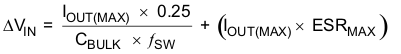
Where IOUT(MAX) is the maximum load current, fSW is the switching frequency, CBULK is the bulk capacitor value and ESRMAX is the maximum series resistance of the bulk capacitor.
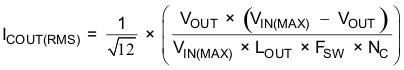
The maximum RMS ripple current also needs to be checked. For worst case conditions, this can be approximated by Equation 7
In this case, the input ripple voltage would be 143 mV and the RMS ripple current would be 1.5 A. It is also important to note that the actual input voltage ripple will be greatly affected by parasitics associated with the layout and the output impedance of the voltage source. The actual input voltage ripple for this circuit is shown in Design Parameters and is larger than the calculated value. This measured value is still below the specified input limit of 300 mV. The maximum voltage across the input capacitors would be VIN max plus ΔVIN/2. The chosen bulk and bypass capacitors are each rated for 50 V and the ripple current capacity is greater than 3 A, both providing ample margin. It is important that the maximum ratings for voltage and current are not exceeded under any circumstance.
9.2.2.4 Output Filter Components
Two components need to be selected for the output filter, L1 and C9. Since the TPS54233 is an externally compensated device, a wide range of filter component types and values can be supported.
9.2.2.4.1 Inductor Selection
To calculate the minimum value of the output inductor, use Equation 8
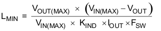
KIND is a coefficient that represents the amount of inductor ripple current relative to the maximum output current. This value is at the discretion of the designer; however, the following guidelines may be used. For designs using low ESR output capacitors such as ceramics, a value as high as KIND = 0.3 may be used. When using higher ESR output capacitors, KIND = 0.2 yields better results.
For this design example, use KIND = 0.3 and the minimum inductor value is calculated to be 14.97μH. For this design, the closest value 15μH was chosen.
For the output filter inductor, it is important that the RMS current and saturation current ratings not be exceeded. The RMS inductor current can be found from Equation 9
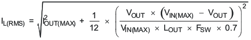
and the peak inductor current can be determined with Equation 10
For this design, the RMS inductor current is 2.02 A and the peak inductor current is 2.43 A. The chosen inductor is a Coilcraft MSS1038-153ML 15 μH. It has a saturation current rating of 3.86 A and an RMS current rating of 3.8 A, meeting these requirements. Smaller or larger inductor values can be used depending on the amount of ripple current the designer wishes to allow so long as the other design requirements are met. Larger value inductors will have lower ac current and result in lower output voltage ripple, while smaller inductor values will increase ac current and output voltage ripple. Inductor values for use with the TPS54233 are in the range of 6.8 μH to 47 μH.
9.2.2.4.2 Capacitor Selection
The important design factors for the output capacitor are dc voltage rating, ripple current rating, and equivalent series resistance (ESR). The dc voltage and ripple current ratings cannot be exceeded. The ESR is important because along with the inductor current it determines the amount of output ripple voltage. The actual value of the output capacitor is not critical, but some practical limits do exist. Consider the relationship between the desired closed loop crossover frequency of the design and LC corner frequency of the output filter. In general, it is desirable to keep the closed loop crossover frequency at less than 1/5 of the switching frequency. With high switching frequencies such as the 300 kHz frequency of this design, internal circuit limitations of the TPS54233 limit the practical maximum crossover frequency to about 25 kHz. In general, the closed loop crossover frequency should be higher than the corner frequency determined by the load impedance and the output capacitor. This limits the minimum capacitor value for the output filter to:
Where RO is the output load impedance (VO/IO) and fCO is the desired crossover frequency. For a desired maximum crossover of 25 kHz the minimum value for the output capacitor is around 3.8μF. This may not satisfy the output ripple voltage requirement. The output ripple voltage consists of two components; the voltage change due to the charge and discharge of the output filter capacitance and the voltage change due to the ripple current times the ESR of the output filter capacitor. The output ripple voltage can be estimated by:
Where NC is the number of output capacitors in parallel.
The maximum ESR of the output capacitor is determined by the amount of allowable output ripple as specified in the initial design parameters; so the maximum specified ESR as listed in the capacitor data sheet is given by Equation 13:
Where ΔVp-p is the desired peak-to-peak output ripple.
To meet the 100 mV p-p ripple requirement, a single 470 μF aluminum electrolytic output capacitor is chosen for C9. This is a Panasonic, EEVFK1A471P rated at 10 V with a maximum ESR of 160 mΩ and a ripple current rating of 600 mA.
The maximum RMS output ripple current can be calculated using Equation 14
The calculated total RMS ripple current is 216 mA and the maximum total ESR required is 43 mΩ. These output capacitors exceed the requirements by a wide margin and will result in a reliable, high-performance design. The selected output capacitor must be rated for a voltage greater than the desired output voltage plus = the ripple voltage. Any derating amount must also be included.
Other capacitor types work well with the TPS54233, depending on the needs of the application.
9.2.2.5 Compensation Components
The external compensation used with the TPS54233 allows for a wide range of output filter configurations. A large range of capacitor values and types of dielectric are supported. The design example uses ceramic X5R dielectric output capacitors, but other types are supported.
A Type II compensation scheme is recommended for the TPS54233. The compensation components are chosen to set the desired closed loop cross over frequency and phase margin for output filter components. The type II compensation has the following characteristics; a dc gain component, a low frequency pole, and a mid frequency zero / pole pair.
The dc gain is determined by Equation 15:
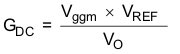
Where:
Vggm = 800
VREF = 0.8 V
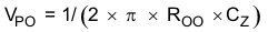
The low-frequency pole is determined by Equation 16:
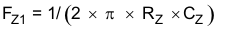
The mid-frequency zero is determined by Equation 17:
And, the mid-frequency pole is given by Equation 18:
The first step is to choose the closed loop crossover frequency. In general, the closed-loop crossover frequency should be less than 1/8 of the minimum operating frequency, but for the TPS54233it is recommended that the maximum closed loop crossover frequency be not greater than 25 kHz. Next, the required gain and phase boost of the crossover network needs to be calculated. By definition, the gain of the compensation network must be the inverse of the gain of the modulator and output filter. For this design example, where the ESR zero is less than the closed loop crossover frequency, the gain of the modulator and output filter can be approximated by Equation 19:
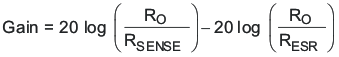
Where:
RSENSE = 1Ω/9
RO = VO/IO
RESR = Equivalent series resistance of the output capacitor
The phase loss is given by Equation 20:

Where:
RESR = Equivalent series resistance of the output capacitor
RO = VO/IO
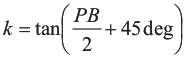
Now that the phase loss is known the required amount of phase boost to meet the phase margin requirement can be determined. The required phase boost is given by Equation 21:

Where PM = the desired phase margin.
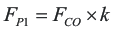
A zero / pole pair of the compensation network will be placed symmetrically around the intended closed loop frequency to provide maximum phase boost at the crossover point. The amount of separation can be determined by Equation 22 and the resultant zero and pole frequencies are given by Equation 23 and Equation 24

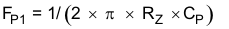
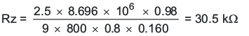
The low-frequency pole is set so that the gain at the crossover frequency is equal to the inverse of the gain of the modulator and output filter. Due to the relationships established by the pole and zero relationships, the value of RZ can be derived directly by Equation 25 :
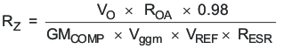
Where:
VO = Output voltage
ROA = 8.696 MΩ
GMCOMP = 9 A/V
Vggm = 800
VREF = 0.8 V
RESR = Equivalent series resistance of the output capacitor
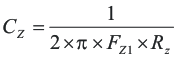
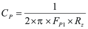
With RZ known, CZ and CP can be calculated using Equation 26 and Equation 27:
For this design, a singe 470 μF output capacitor is used. The ESR is approximately .160 Ω. The desired closed loop crossover frequency is 22000 Hz.
Using Equation 19 and Equation 20, the output stage gain and phase loss are equivalent as:
Gain = –3.114 dB
and
PL = –4.96 degrees
For 60 degrees of phase margin, Equation 21 requires no additional phase boost, so K can be set equal to 1.
Equation 22, Equation 23, and Equation 24 are used to find the zero and pole frequencies of:
FZ1 = 22000 Hz
And
FP1 = 22000 Hz
RZ, CZ, and CP are calculated using Equation 25, Equation 26, and Equation 27:
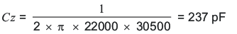
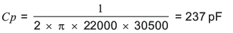
Using standard values for R3, C6, and C7 in the application schematic of Figure 12:
R3 = 30.9 kΩ
C6 = 220 pF
C7 = 220 pF
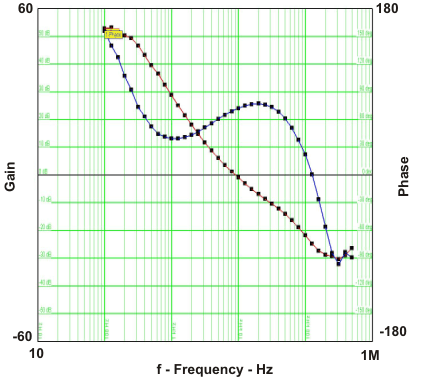
The measured overall loop response for the circuit is given in Figure 12. Note that the actual closed loop crossover frequency is higher than intended at about 25 kHz. This is primarily due to variation in the actual values of the output filter components and tolerance variation of the internal feed-forward gain circuitry. Overall the design has greater than 60 degrees of phase margin and will be completely stable over all combinations of line and load variability.
9.2.2.6 Bootstrap Capacitor
Every TPS54233 design requires a bootstrap capacitor, C4. The bootstrap capacitor must be 0.1 μF. The bootstrap capacitor is located between the PH pins and BOOT pin. The bootstrap capacitor should be a high-quality ceramic type with X7R or X5R grade dielectric for temperature stability.
9.2.2.7 Catch Diode
The TPS54233 is designed to operate using an external catch diode between PH and GND. The selected diode must meet the absolute maximum ratings for the application: Reverse voltage must be higher than the maximum voltage at the PH pin, which is VINMAX + 0.5 V. Peak current must be greater than IOUTMAX plus on half the peak to peak inductor current. Forward voltage drop should be small for higher efficiencies. It is important to note that the catch diode conduction time is typically longer than the high-side FET on time, so attention paid to diode parameters can make a marked improvement in overall efficiency. Additionally, check that the device chosen is capable of dissipating the power losses. For this design, a Diodes, Inc. B340A is chosen, with a reverse voltage of 40 V, forward current of 3 A, and a forward voltage drop of 0.5 V.
9.2.2.8 Output Voltage Limitations
Due to the internal design of the TPS54233, there are both upper and lower output voltage limits for any given input voltage. The upper limit of the output voltage set point is constrained by the maximum duty cycle of 91% and is given by Equation 31:

Where:
VIN min = Minimum input voltage
IO max = Maximum load current
VD = Catch diode forward voltage
RL = Output inductor series resistance
The equation assumes maximum on resistance for the internal high-side FET.
The lower limit is constrained by the minimum controllable on time which may be as high as 160 ns. The approximate minimum output voltage for a given input voltage and minimum load current is given by Equation 32:

Where:
VIN max = Maximum input voltage
IO min = Minimum load current
VD = Catch diode forward voltage
RL = Output inductor series resistance
This equation assumes nominal on-resistance for the high-side FET and accounts for worst case variation of operating frequency set point. Any design operating near the operational limits of the device should be carefully checked to assure proper functionality.
9.2.2.9 Power Dissipation Estimate
The following formulas show how to estimate the device power dissipation under continuous conduction mode operations. They should not be used if the device is working in the discontinuous conduction mode (DCM) or pulse skipping Eco-modeTM.
The device power dissipation includes:
1) Conduction loss: Pcon = Iout2 x RDS(on) x VOUT/VIN
2) Switching loss: Psw = 0.5 x 10⁻⁹ x VIN2 x IOUT x Fsw
3) Gate charge loss: Pgc = 22.8 x 10⁻⁹ x Fsw
4) Quiescent current loss: Pq = 0.075 x 10⁻³ x VIN
Where:
IOUT is the output current (A).
RDS(on) is the on-resistance of the high-side MOSFET (Ω).
VOUT is the output voltage (V).
VIN is the input voltage (V).
Fsw is the switching frequency (Hz).
So
Ptot = Pcon + Psw + Pgc + Pq
For given TA , TJ = TA + Rth x Ptot.
For given TJMAX = 150°C, TAMAX = TJMAX– Rth x Ptot.
Where:
Ptot is the total device power dissipation (W).
TA is the ambient temperature (°C).
TJ is the junction temperature (°C) .
Rth is the thermal resistance of the package (°C/W).
TJMAX is maximum junction temperature (°C).
TAMAX is maximum ambient temperature (°C).
9.2.3 Application Curves
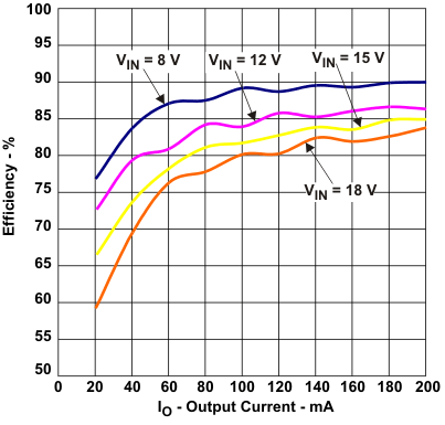
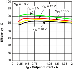
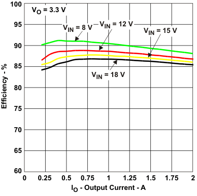 Figure 13. TPS54233 Efficiency
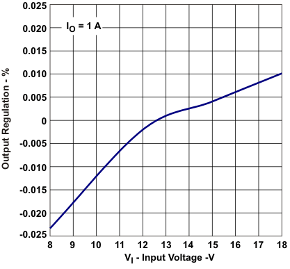
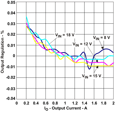 Figure 15. TPS54233 Load Regulation
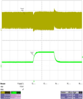 Figure 17. TPS54233 Transient Response
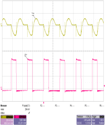 Figure 19. TPS54233 Input Ripple
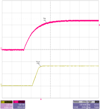 Figure 21. TPS54233 Start Up
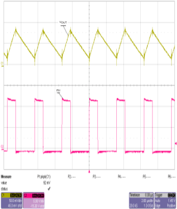
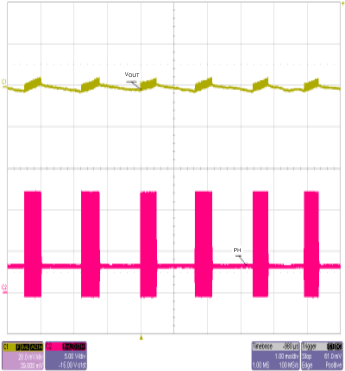 Figure 23. TPS54233 Eco-mode™ Operation