SLUSA44A March 2010 – July 2015 BQ24640
PRODUCTION DATA.
- 1 Features
- 2 Applications
- 3 Description
- 4 Revision History
- 5 Pin Configuration and Functions
- 6 Specifications
-
7 Detailed Description
- 7.1 Overview
- 7.2 Functional Block Diagram
- 7.3
Feature Description
- 7.3.1 Output Voltage Regulation
- 7.3.2 Output Current Regulation
- 7.3.3 Power Up
- 7.3.4 Enable and Disable Charging
- 7.3.5 Automatic Internal Soft-Start Charger Current
- 7.3.6 Converter Operation
- 7.3.7 Synchronous and Nonsynchronous Operation
- 7.3.8 Input Overvoltage Protection (ACOV)
- 7.3.9 Output Overvoltage Protection
- 7.3.10 Cycle-by-Cycle Charge Overcurrent Protection
- 7.3.11 Thermal Shutdown Protection
- 7.3.12 Temperature Qualification
- 7.3.13 CE (Charge Enable)
- 7.3.14 PG Output
- 7.3.15 Charge Status Outputs
- 7.4 Device Functional Modes
- 8 Application and Implementation
- 9 Power Supply Recommendations
- 10Layout
- 11Device and Documentation Support
- 12Mechanical, Packaging, and Orderable Information
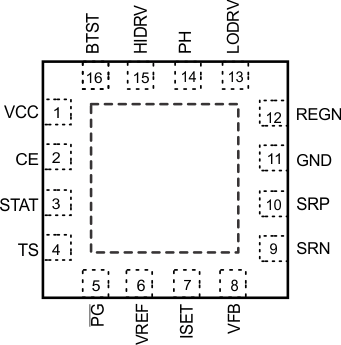
5 Pin Configuration and Functions
RVA Package
16-Pin VQFN With Exposed Thermal Pad
Top View

Pin Functions
| PIN | TYPE(1) | DESCRIPTION | |
|---|---|---|---|
| NAME | NO. | ||
| BTST | 16 | P | PWM high-side driver positive supply. Connect the 0.1-μF bootstrap capacitor from PH to BTST. |
| CE | 2 | I | Charge enable, active HIGH logic input. HI enables charge, and LO disables charge. Connect to pullup rail with 10-kΩ resistor. It has an internal 1-MΩ pulldown resistor. |
| GND | 11 | P | Low-current sensitive analog/digital ground. On PCB layout, connect with thermal pad underneath the IC. |
| HIDRV | 15 | O | PWM high-side driver output. Connect to the gate of the high-side N-channel power MOSFET with a short trace. |
| ISET | 7 | I | Charge current set point. The voltage is set through a voltage divider from VREF to ISET and to GND. |
| LODRV | 13 | O | PWM low-side driver output. Connect to the gate of the low-side N-channel power MOSFET with a short trace. |
| PG | 5 | O | Open-drain active-low adapter status output. Connect to pullup rail through LED and 10-kΩ resistor. The LED turns on when a valid is detected, and off in the sleep mode. |
| PH | 14 | P | Switching node, charge current output inductor connection. Connect the 0.1-μF bootstrap capacitor from PH to BTST. |
| REGN | 12 | P | PWM low-side driver positive 6-V supply output. Connect a 1-μF ceramic capacitor from REGN to GND pin close to the IC. Use for low-side driver and high-side driver bootstrap voltage by small signal Schottky diode from REGN to BTST. |
| SRN | 9 | I | Charge current-sense resistor, negative input. A 0.1-μF ceramic capacitor is placed from SRN to SRP to provide differential-mode filtering. An optional 0.1-μF ceramic capacitor is placed from SRN pin to GND for common-mode filtering. |
| SRP | 10 | P/I | Charge current sense resistor, positive input. A 0.1-μF ceramic capacitor is placed from SRN to SRP to provide differential-mode filtering. A 0.1-μF ceramic capacitor is placed from SRP pin to GND for common-mode filtering. |
| STAT | 3 | O | Open-drain charge status output to indicate various charger operation. Connect to the pullup rail through the LED and 10-kΩ (see Table 4). |
| TS | 4 | I | Temperature qualification voltage input for negative temperature coefficient thermistor. Program the hot and cold temperature window with a resistor-divider from VREF to TS to GND. Recommend SEMITEC 103AT-2 10-kΩ thermister. |
| VCC | 1 | P | IC power positive supply. Connect through a 10-Ω resistor to the cathode of input diode. Place a 1-μF ceramic capacitor from VCC to GND and place it as close as possible to IC to filter out the noise. |
| VFB | 8 | I | Charge voltage analog feedback adjustment. Connect a resistor divider from output to VFB to GND to adjust the output voltage. The internal regulation limit is 2.1V. |
| VREF | 6 | P | 3.3-V reference voltage output. Place a 1-μF ceramic capacitor from VREF to GND pin close to the IC. This voltage could be used for programming charge current regulation on ISET and for thermal threshold on TS. It can be used as the pullup rail of STAT, and PG. |
| Thermal pad | — | Exposed pad beneath the IC. Always solder thermal pad to the board, and have vias on the thermal pad plane star-connecting to GND and ground plane for high-current power converter. It also serves as a thermal pad to dissipate the heat. | |
(1) P - Power, I - Input, O - Output