SLUSAM9E July 2011 – April 2020
PRODUCTION DATA.
- 1 Features
- 2 Applications
- 3 Description
- 4 Revision History
- 5 Description (Continued)
- 6 Pin Configuration and Functions
-
7 Specifications
- 7.1 Absolute Maximum Ratings
- 7.2 ESD Ratings
- 7.3 Recommended Operating Conditions
- 7.4 Thermal Information
- 7.5 Electrical Characteristics: Supply Current
- 7.6 Internal Power Control (Startup and Shutdown)
- 7.7 3.3-V Voltage Regulator
- 7.8 Voltage Reference
- 7.9 Cell Voltage Amplifier
- 7.10 Current Sense Amplifier
- 7.11 Overcurrent Comparator
- 7.12 Internal Temperature Measurement
- 7.13 Cell Balancing and Open Cell Detection
- 7.14 I2C Compatible Interface
- 7.15 Typical Characteristics
-
8 Detailed Description
- 8.1 Overview
- 8.2 Functional Block Diagram
- 8.3 Feature Description
- 8.4 Device Functional Modes
- 8.5 Programming
- 8.6 Register Maps
- 9 Application and Implementation
- 10Power Supply Recommendations
- 11Layout
- 12Device and Documentation Support
- 13Mechanical, Packaging, and Orderable Information
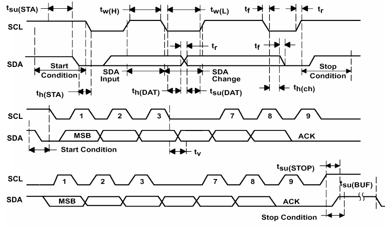
7.14 I2C Compatible Interface
| PARAMETERS | MIN | TYP | MAX | UNIT | ||
|---|---|---|---|---|---|---|
| DC PARAMETERS | ||||||
| VIL | Input Low Logic Threshold | 0.6 | V | |||
| VIH | Input High Logic Threshold | 2.8 | V | |||
| VOL | Output Low Logic Drive | IOL = 1 mA | 0.20 | V | ||
| IOL = 2.5 mA | 0.40 | |||||
| VOH | Output High Logic Drive (Not applicable due to open-drain outputs) | N/A | V | |||
| ILKG | I2C Pin Leakage | Pin = 5 V, Output in Hi-Z | < 1 | µA | ||
| AC PARAMETERS | ||||||
| tr | SCL, SDA Rise Time | 1000 | ns | |||
| tf | SCL, SDA Fall Time | 300 | ns | |||
| tw(H) | SCL Pulse Width High | 4 | µs | |||
| tw(L) | SCL Pulse Width Low | 4.7 | µs | |||
| tsu(STA) | Setup time for START condition | 4.7 | µs | |||
| th(STA) | START condition hold time after which first clock pulse is generated | 4 | µs | |||
| tsu(DAT) | Data setup time | 250 | ns | |||
| th(DAT) | Data hold time | 0(1) | µs | |||
| tsu(STOP) | Setup time for STOP condition | 4 | µs | |||
| tsu(BUF) | Time the bus must be free before new transmission can start | 4.7 | µs | |||
| t V | Clock Low to Data Out Valid | 900 | ns | |||
| th(CH) | Data Out Hold Time After Clock Low | 0 | ns | |||
| fSCL | Clock Frequency | 0 | 100 | kHz | ||
| tWAKE | I2C ready after transition to Wake Mode | 2.5 | ms | |||
(1) Devices must provide internal hold time of at least 300 ns for the SDA signal-to-bridge of the undefined region of the falling edge of SCL.
 Figure 1. I2C Timing