SLUSCO1B June   2017  – July 2024 UCC27212

PRODUCTION DATA  

  1.   1
  2. Features
  3. Applications
  4. Description
  5. Pin Configuration and Functions
  6. Specifications
    1. 5.1 Absolute Maximum Ratings
    2. 5.2 ESD Ratings
    3. 5.3 Recommended Operating Conditions
    4. 5.4 Thermal Information
    5. 5.5 Electrical Characteristics
    6. 5.6 Switching Characteristics
    7. 5.7 Timing Diagrams
    8. 5.8 Typical Characteristics
  7. Detailed Description
    1. 6.1 Overview
    2. 6.2 Functional Block Diagram
    3. 6.3 Feature Description
      1. 6.3.1 Input Stages
      2. 6.3.2 Undervoltage Lockout (UVLO)
      3. 6.3.3 Level Shift
      4. 6.3.4 Boot Diode
      5. 6.3.5 Output Stages
    4. 6.4 Device Functional Modes
  8. Application and Implementation
    1. 7.1 Application Information
    2. 7.2 Typical Application
      1. 7.2.1 Design Requirements
      2. 7.2.2 Detailed Design Procedure
        1. 7.2.2.1 Power Dissipation
      3. 7.2.3 Application Curves
  9. Power Supply Recommendations
  10. Layout
    1. 9.1 Layout Guidelines
    2. 9.2 Layout Example
      1. 9.2.1 Thermal Considerations
  11. 10Device and Documentation Support
    1. 10.1 Device Support
      1. 10.1.1 Third-Party Products Disclaimer
    2. 10.2 Documentation Support
      1. 10.2.1 Related Documentation
    3. 10.3 Receiving Notification of Documentation Updates
    4. 10.4 Support Resources
    5. 10.5 Trademarks
    6. 10.6 Electrostatic Discharge Caution
    7. 10.7 Glossary
  12. 11Revision History
  13. 12Mechanical, Packaging, and Orderable Information

Description

The UCC27212 device has a peak output current of 3.7A source and 4.5A sink, which allows for the ability to drive large power MOSFETs. The device features an on-chip 120V rated bootstrap diode eliminating the need for external discrete diodes. The input structure can directly handle –10V, which increases robustness and is also independent of supply voltage. The UCC27212 offers 5V turn-off UVLO which helps lower power losses and increased input hysteresis that allows for interface to analog or digital PWM controllers with enhanced noise immunity. The switching node of the UCC27212 (HS pin) can handle –(24 – VDD)V maximum, which allows the high-side channel to be protected from inherent negative voltages.

Device Information
PART NUMBERPACKAGE(1)BODY SIZE (NOM)
UCC27212DPR (WSON, 10)4.00mm x 4.00mm
For all available packages, see the orderable addendum at the end of the data sheet.
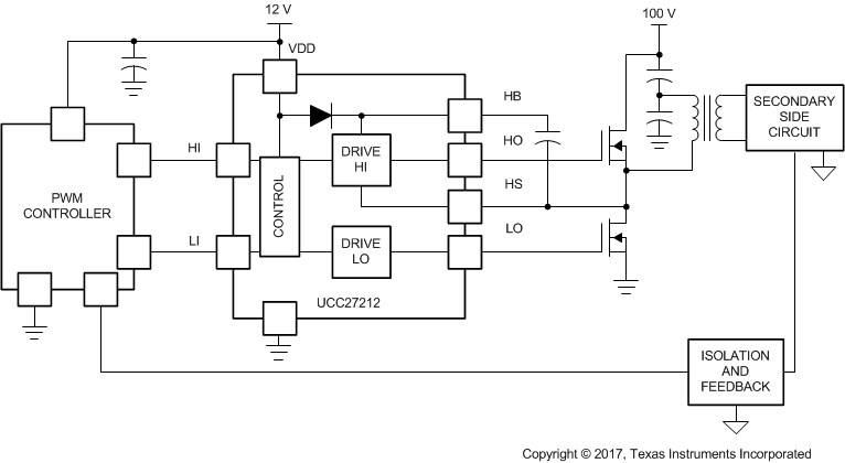
UCC27212 Typical Application
                        DiagramTypical Application Diagram
UCC27212 Propagation Delays vs Supply Voltage T =
                        25°CPropagation Delays vs Supply Voltage T = 25°C