SLUSDG3F August 2018 – September 2024
PRODUCTION DATA
- 1
- 1 Features
- 2 Applications
- 3 Description
- 4 Pin Configuration and Functions
-
5 Specifications
- 5.1 Absolute Maximum Ratings
- 5.2 ESD Ratings (Automotive)
- 5.3 Recommended Operating Conditions
- 5.4 Thermal Information
- 5.5 Power Ratings
- 5.6 Insulation Specifications
- 5.7 Safety Limiting Values
- 5.8 Electrical Characteristics
- 5.9 Timing Requirements
- 5.10 Switching Characteristics
- 5.11 Insulation Characteristics Curves
- 5.12 Typical Characteristics
- 6 Parameter Measurement Information
- 7 Detailed Description
-
8 Application and Implementation
- 8.1 Application Information
- 8.2
Typical Application
- 8.2.1 Design Requirements
- 8.2.2 Detailed Design Procedure
- 8.2.3 Application Curves
- 9 Power Supply Recommendations
- 10Layout
- 11Device and Documentation Support
- 12Revision History
- 13Mechanical, Packaging, and Orderable Information
4 Pin Configuration and Functions
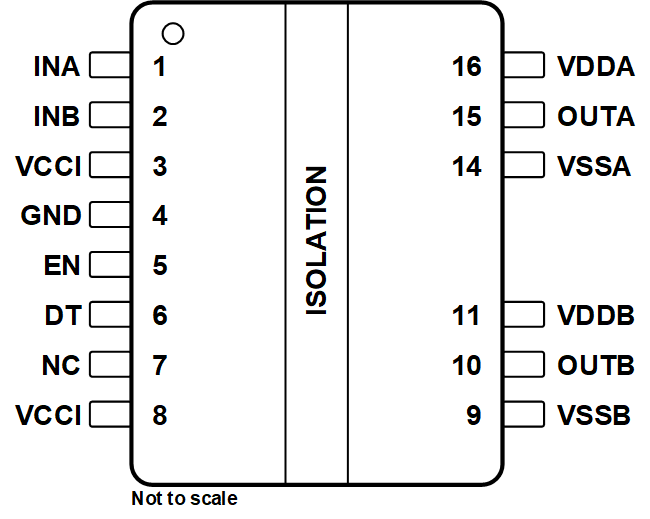
 Figure 4-1 DWK Package, 14-Pin SOIC (Top View)
Table 4-1 Pin Functions
| PIN | TYPE(1) | DESCRIPTION | |
|---|---|---|---|
| NAME | NO. | ||
| DT | 6 | I | DT
pin configuration:
|
| EN | 5 | I | Enable both driver outputs if asserted high, disable the output if set low. It is recommended to tie this pin to VCCI if not used to achieve better noise immunity. Bypass using a ≈ 1-nF low ESR/ESL capacitor close to EN pin when connecting to a micro controller with distance. |
| GND | 4 | P | Primary-side ground reference. All signals in the primary side are referenced to this ground. |
| INA | 1 | I | Input signal for A channel. INA input has a TTL/CMOS compatible input threshold. This pin is pulled low internally if left open. It is recommended to tie this pin to ground if not used to achieve better noise immunity. |
| INB | 2 | I | Input signal for B channel. INB input has a TTL/CMOS compatible input threshold. This pin is pulled low internally if left open. It is recommended to tie this pin to ground if not used to achieve better noise immunity. |
| NC | 7 | – | No internal connection. This pin can be left floating, tied to VCCI, or tied to GND. |
| OUTA | 15 | O | Output of driver A. Connect to the gate of the A channel FET or IGBT. |
| OUTB | 10 | O | Output of driver B. Connect to the gate of the B channel FET or IGBT. |
| VCCI | 3 | P | Primary-side supply voltage. Locally decoupled to GND using a low ESR/ESL capacitor located as close to the device as possible. |
| VCCI | 8 | P | Primary-side supply voltage. This pin is internally shorted to pin 3. |
| VDDA | 16 | P | Secondary-side power for driver A. Locally decoupled to VSSA using a low ESR/ESL capacitor located as close to the device as possible. |
| VDDB | 11 | P | Secondary-side power for driver B. Locally decoupled to VSSB using low ESR/ESL capacitor located as close to the device as possible. |
| VSSA | 14 | P | Ground for secondary-side driver A. Ground reference for secondary side A channel. |
| VSSB | 9 | P | Ground for secondary-side driver B. Ground reference for secondary side B channel. |
(1) P =Power, I= Input, O= Output