SLUUBM0D May   2017  – October 2020 TPS92518 , TPS92518-Q1 , TPS92518HV , TPS92518HV-Q1


  1.   Trademarks
  2. 1Description
    1. 1.1 Typical Applications
    2. 1.2 Connector Description
  3. 2Performance Specifications
  4. 3Performance Data and Typical Characteristic Curves
    1. 3.1 Startup Waveforms
      1. 3.1.1 Startup After SPI Enable Command
      2. 3.1.2 Startup on Hardware Enable Pin Transition
    2. 3.2 Shutdown Waveforms
      1. 3.2.1 Shutdown After SPI Disable
      2. 3.2.2 Shutdown After Hardware Enable Pin Transition
    3. 3.3 Current Sharing
    4. 3.4 Diode and Boot Capacitor Current
      1. 3.4.1 Diode, Inductor, and Boot Capacitor Current at Low Output Current
      2. 3.4.2 Diode, Inductor, and Boot Capacitor Current at High Output Current
      3. 3.4.3 Shunt FET Dimming
      4. 3.4.4 Undervoltage Lockout Description
  5. 4Schematic, PCB Layout, and Bill of Materials
    1. 4.1 Schematic
    2. 4.2 Layout
    3. 4.3 Bill of Materials
  6. 5Software
    1. 5.1 TPS92518 Demonstration Kit Software Installation
      1. 5.1.1 Windows 10
  7. 6Use of LEDSPIMCUEVM-879 Microcontroller Board for SPI Communications with the TPS92518
  8. 7Revision History

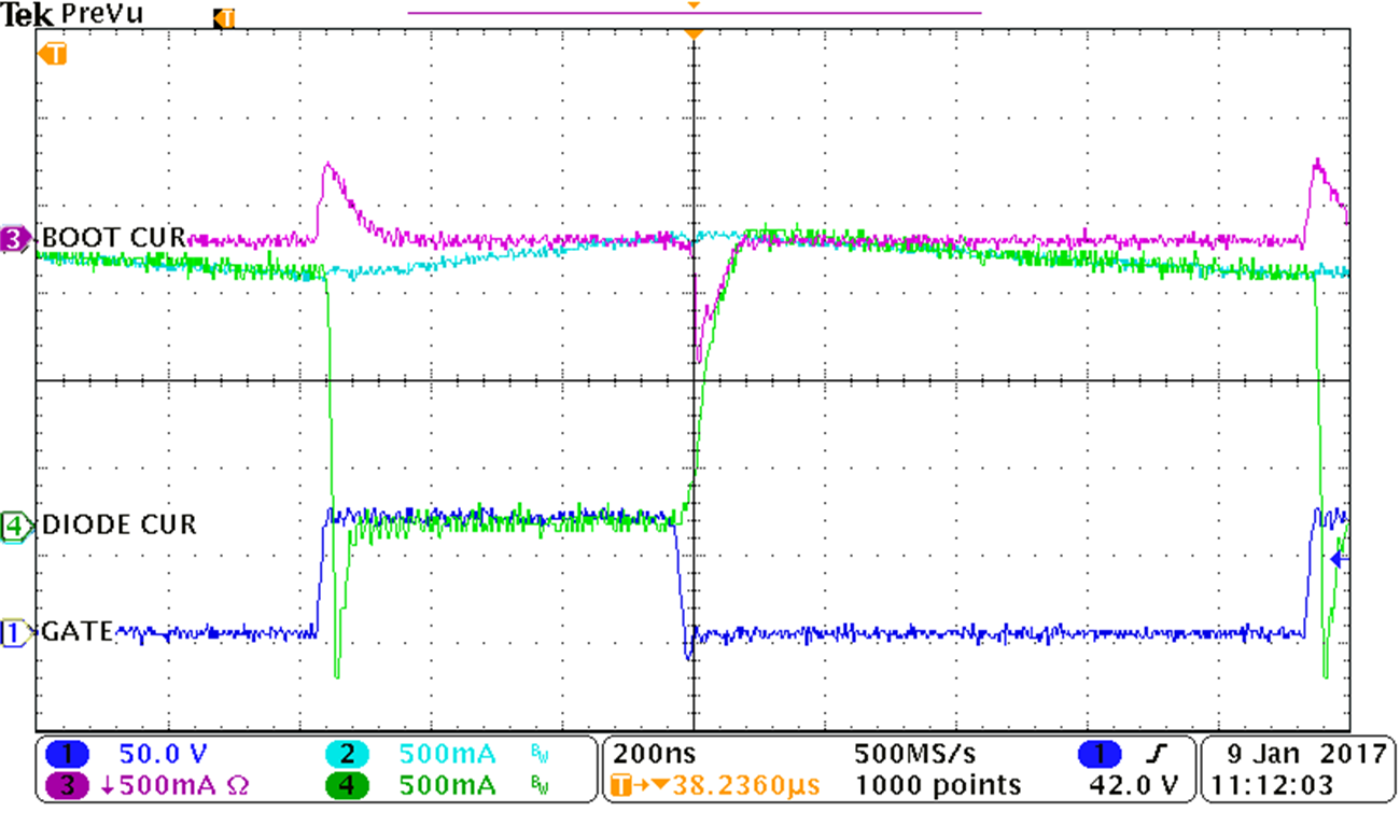
Diode, Inductor, and Boot Capacitor Current at High Output Current

GUID-23664874-9750-4ADD-A1D4-A533B4F0F073-low.png
Showing inductor current into the LED and current flow through the catch diode and boot capacitor used for supplying gate drive power. VIN = 65  V, VLED = 23 V, TOFF register setting 50, peak threshold register setting = 1
Figure 3-11 Switch Node Current