SLUUCC4A October   2020  – September 2021 TPS92520-Q1


  1.   Trademarks
  2.   General Texas Instruments High Voltage Evaluation (TI HV EMV) User Safety Guidelines
  3. 1Description
    1. 1.1 Typical Applications
    2. 1.2 Warnings
    3. 1.3 Connector Description
  4. 2Performance Specifications
  5. 3Performance Data and Typical Characteristic Curves
    1. 3.1 1.5A CC BUCK SW-Node Voltage Waveform
    2. 3.2 Start-up Waveforms
    3. 3.3 PWM Dimming
  6. 4Schematic, PCB Layout, and Bill of Materials
    1. 4.1 Schematic
    2. 4.2 Layout
    3. 4.3 Bill of Materials
  7. 5Software
    1. 5.1 Demonstration Kit Software Installation for LEDMCUEVM-132 Board
      1. 5.1.1 Installation Overview
    2. 5.2 Step-by-Step Installation Instructions
    3. 5.3 Installation Error Recovery
    4. 5.4 Checking for Updates
  8. 6TPS92520EVM-133 Power Up and Operation
    1. 6.1 Power Up and Operation at VINx < 40 V
    2. 6.2 MCU Control Window
    3. 6.3 SPI Command Window
    4. 6.4 Watchdog Window
    5. 6.5 GUI Devices Window
      1. 6.5.1 Channel 1 or 2 Sub-Window: Settings, Measurements, and Faults
      2. 6.5.2 Device Sub-Window: Shared Device Settings, Measurements, Register Info, and Limp Home
    6. 6.6 Limp Home Mode Window
  9. 7Revision History

Channel 1 or 2 Sub-Window: Settings, Measurements, and Faults

The Channel Sub-Window is broken down into basic features and settings set by selecting boxes or slide, measurements of VIN and LED, and fault status boxes (see Figure 6-20).
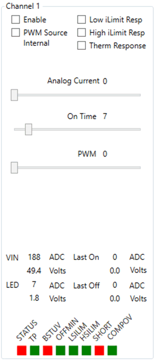
GUID-20200824-CA0I-RX7N-3TNL-FZNJMSK87S8D-low.gifFigure 6-20 Channel 1 Window - Configurations, Measurement, and Fault Window.
There are three slide bars that can be adjusted. The Analog Current bar sets the CHxIADJ registers to control the reference voltage (VIADJ) used for setting the LED current of that channel. It has a decimal value from 0 to 1023, which coincides with voltage from 0 to 2.45 V to the V-I Converter, see the LED Current Regulation and Error Amplifier section of the TPS92520-Q1 data sheet for additional information. The current setpoint is also a function of the selected current sense resistor. The TPS92520EVM-133 uses a 100-mΩ resistor and to get 1 A at the output then slide bar must be move to 586 (decimal value), see Figure 6-21.

GUID-20200908-CA0I-4XL4-GTS6-PBDFDTXVSWZ2-low.gifFigure 6-21 Analog Current Slide Bar.

The On Time slide adjust CHxTON registers which controls the switching frequency of the constant current LED buck driver, see Figure 6-22. The default value is 7 (decimal) which coincides with a 437-kHz switching frequency. The switching frequency ranges from 100 kHz to 2,200 kHz, see the Switching Frequency and Adaptive On-Time Control section of the TPS92520-Q1 data sheet for detailed calculations. The EVM is optimized to operate at the default switching frequency.

GUID-20200908-CA0I-P0HV-VC1G-FCDPXB9MSKXL-low.gifFigure 6-22 On Time Slide Bar for Changing Switching Frequency.

The PWM slide adjusts the internal 10 bit PWM duty cycle (CHxPWM registers) from 0 to 1023, which coincides with 0 (off) and 1023 (full ON), see Figure 6-23. For example, if you want to operate at a 50% duty cycle slide the bar to 512 (decimal value), which is half of the full scale of 1024 or 50%. The PWM Source Internal box much be selected for the PWM slide bar setting to be implemented. The PWM Source Internal box sets the CHxINTPWM bit high and enables the use of the internal PWM registers to generate the PWM function for that channel.

GUID-20200908-CA0I-ZT38-PQ41-FDDPV7RVQF5D-low.gifFigure 6-23 Internal PWM Duty Cycle Slide Bar.

The Enable box set the CHxEN bit to 1 for that channel, which means the associated channel is turned on, see Figure 6-24.

GUID-20200908-CA0I-DHWC-9VX1-5577ZXC1RVFP-low.gifFigure 6-24 Channel Feature Selection Boxes.
The PWM Source Internal controls the CHxINTPWM register. If the box is selected then the device uses the register settings for PWM slide bar to determine the PWM duty cycle and uses the PWMDIV register to set the PWM frequency. Note that the PWM frequency (PWMDIV register) sets the frequency for both channels. If this box is not selected then then the device does PWM dimming based on the signal seen on the UDIM x pins for each respective channel. The frequency and duty cycle are independent.

The Low iLimit Resp, High iLimit Resp, and Therm Response buttons coincide with setting the device to auto-restart after a fault time (IFT register setting) has elapsed or if it will latch off when the fault occurs. If box is selected then the device will latch off when the fault occurs and then reset the EN bit to the default of 0 (off) and will only continue to run when the EN bit is set to 1 (enabled).

Each channel window also reads the input voltage (VIN) and the output LED voltage (LED) at the CSNx pin for each respective channel using the internal ADC of the device. VIN is a reading of the CHxVIN registers and LED is a reading of CHxVLED registers, see Figure 6-25.
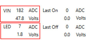
GUID-20200908-CA0I-JPBH-Q76Z-XSBP8XK2PBXD-low.gifFigure 6-25 VIN and LED Voltage Measurements From Internal ADC.
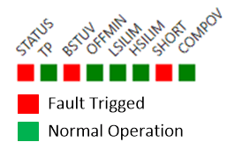
At the bottom of the channel window are several boxes, that are either red or green, that indicate the status of specific warnings or faults, see Figure 6-26. The STATUS box reads the CHxSTATUS bit and is logic OR of all the fault bits for that channel with the exception of the overtemperature thermal warning bit. The "TP" box reads the CHxTP bit and indicates overtemperature thermal protection for that channel. The BSTUV box reads the CHxBSTUV bit and indicates the boostrap undervoltage fault condition where the BSTx voltage is less than 2.95 V. The OFFMIN box reads the CHxOFFMIN bit and indicates if the maximum duty cycle of that channel has been reached. The LSILIM box reads the CHxLSILM bit and indicates that the low-side switch current limit fault has occurred on that channel, which is 1.5 A typical. The HSILIM box reads the CHxHSILIM bit and indicates that the high-side switch current limit fault has occurred on that channel, which is 2.7 A typical. The SHORT box reads the CHxSHORT bit and indicates output short circuit fault on that channel, which means the CSPx pin is less than 2.45 V. The COMPOV box reads the CHxSHORT bit for each channel and indicates that an overvoltage condition on the COMPx pin, which indicates the COMPx pin is greater than 3.2 V.
GUID-20200908-CA0I-CRWG-RKSD-ZVVPXQPV6VGG-low.gifFigure 6-26 Status Indicators for Channels.