SLUUCC4A October   2020  – September 2021 TPS92520-Q1


  1.   Trademarks
  2.   General Texas Instruments High Voltage Evaluation (TI HV EMV) User Safety Guidelines
  3. 1Description
    1. 1.1 Typical Applications
    2. 1.2 Warnings
    3. 1.3 Connector Description
  4. 2Performance Specifications
  5. 3Performance Data and Typical Characteristic Curves
    1. 3.1 1.5A CC BUCK SW-Node Voltage Waveform
    2. 3.2 Start-up Waveforms
    3. 3.3 PWM Dimming
  6. 4Schematic, PCB Layout, and Bill of Materials
    1. 4.1 Schematic
    2. 4.2 Layout
    3. 4.3 Bill of Materials
  7. 5Software
    1. 5.1 Demonstration Kit Software Installation for LEDMCUEVM-132 Board
      1. 5.1.1 Installation Overview
    2. 5.2 Step-by-Step Installation Instructions
    3. 5.3 Installation Error Recovery
    4. 5.4 Checking for Updates
  8. 6TPS92520EVM-133 Power Up and Operation
    1. 6.1 Power Up and Operation at VINx < 40 V
    2. 6.2 MCU Control Window
    3. 6.3 SPI Command Window
    4. 6.4 Watchdog Window
    5. 6.5 GUI Devices Window
      1. 6.5.1 Channel 1 or 2 Sub-Window: Settings, Measurements, and Faults
      2. 6.5.2 Device Sub-Window: Shared Device Settings, Measurements, Register Info, and Limp Home
    6. 6.6 Limp Home Mode Window
  9. 7Revision History

Limp Home Mode Window

The TPS92520-Q1 enters the limp home mode of operation after detecting three consecutive watchdog timeout events or when the LHSW bit is set high in the SYSCFG1 register. The limp home mode is programmed by a variety of registers that sets the operational setpoint. By selecting the Limp Home button in the Devices Window it will open up the Limp Home Mode window. The main Limp Home Mode window now appears as shown in Figure 6-31. This window include three sub-windows (Channel 1, Channel 2, and Device). The channel windows have three slide bars that control Analog Current, On Time (switching frequency), and PWM (internal PWM duty cycle). This is setup similarly to the Run Mode windows and adjusts the LHxIADJ registers, the LHxTON registers, and the LHxPWM registers set-points. Similar to the Channel windows in the Run Mode it also has selection boxes for Enable, PWM Source, PWM 100%, Low iLimit Resp, High iLimit Resp, and Therm Response.

Device: The window shows a fault timer that is selectable in ms. A check box sets whether the limp home mode reference point is generated from the LHxIADJ registers for each channel or if the input voltage at the LHI pin sets the reference voltage for both channels. See the Detailed Description section of the TPS92520-Q1 data sheet for more detailed information. The Limp Mode On button sets the LHSW bit in the SYSCFG1 register. This allows to turn on the setting put into the limp home registers without having to go through the conditions that cause the device to go into limp home mode.
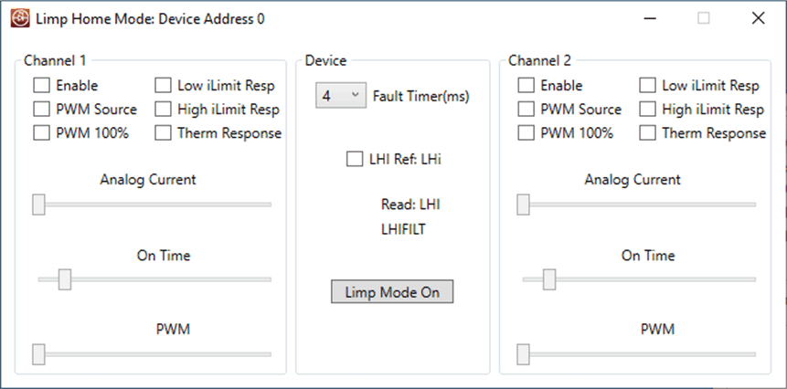
GUID-20200901-CA0I-DWBC-GTJV-F8S96XQ7Z5VR-low.gif Figure 6-31 GUI, Limp Home Mode Window

An example limp home mode is as follows. The Channels are enabled using the enable box. The PWM source box is enabled and it sets the PWM duty cycle references to the slide bar for PWM, which is the internal PWM duty cycle control. The PWM duty cycle is set to 512 out of 1024 scale and is therefore a 50% duty cycle. The On Time slide bar is set to 7, which is the approximately 440-kHz switching frequency. Analog Current is set to 300, which sets the board to output to approximately 519 mA. The Fault Timer is set to 4 ms. The LHI Ref: LHi box is not selected; therefore the reference for limp home is internal.
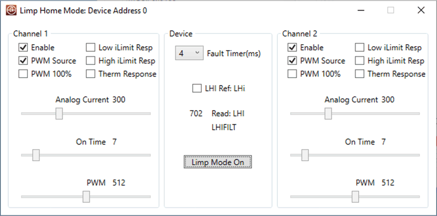
GUID-20200901-CA0I-PXCR-VLCQ-6KN6DVGGSQDX-low.gif Figure 6-32 Example Limp Home Mode Settings.