SLUUCG7 April 2024 BQ76922
- 1
- Read This First
- 1 Introduction
- 2 Device Description
- 3 Device Configuration
-
4 Measurement Subsystem
- 4.1 Voltage Measurement
- 4.2 General Purpose ADCIN Functionality
- 4.3 Coulomb Counter and Digital Filters
- 4.4 Synchronized Voltage and Current Measurement
- 4.5 Subcommands 0x0071–0x0072 DASTATUS1-2() , Cell Voltage and Synchronized Current Counts
- 4.6 Subcommands 0x0075–0x0076 DASTATUS5-6(), Additional Measurements
- 4.7 Internal Temperature Measurement
- 4.8 Thermistor Temperature Measurement
- 4.9 Factory Trim of Voltage ADC
- 4.10 Voltage Calibration (ADC Measurements)
- 4.11 Voltage Calibration (COV and CUV Protections)
- 4.12 Current Calibration
- 4.13 Temperature Calibration
-
5 Primary and Secondary Protection Subsystems
- 5.1 Protections Overview
- 5.2
Primary Protections
- 5.2.1 Primary Protections Overview
- 5.2.2 High-Side NFET Drivers
- 5.2.3 Protection FETs Configuration and Control
- 5.2.4 Cell Overvoltage Protection
- 5.2.5 Cell Undervoltage Protection
- 5.2.6 Short Circuit in Discharge Protection
- 5.2.7 Overcurrent in Charge Protection
- 5.2.8 Overcurrent in Discharge 1, 2, and 3 Protections
- 5.2.9 Overtemperature in Charge Protection
- 5.2.10 Overtemperature in Discharge Protection
- 5.2.11 Overtemperature FET Protection
- 5.2.12 Internal Overtemperature Protection
- 5.2.13 Undertemperature in Charge Protection
- 5.2.14 Undertemperature in Discharge Protection
- 5.2.15 Internal Undertemperature Protection
- 5.2.16 Host Watchdog Protection
- 5.2.17 Precharge Timeout Protection
- 5.2.18 Load Detect Functionality
- 5.3
Secondary Protections
- 5.3.1 Secondary Protections Overview
- 5.3.2 Copper Deposition (CUDEP) Permanent Fail
- 5.3.3 Safety Undervoltage (SUV) Permanent Fail
- 5.3.4 Safety Overvoltage (SOV) Permanent Fail
- 5.3.5 Safety Overcurrent in Charge (SOCC) Permanent Fail
- 5.3.6 Safety Overcurrent in Discharge (SOCD) Permanent Fail
- 5.3.7 Safety Cell Overtemperature (SOT) Permanent Fail
- 5.3.8 Safety FET Overtemperature (SOTF) Permanent Fail
- 5.3.9 Charge FET (CFETF) Permanent Fail
- 5.3.10 Discharge FET (DFETF) Permanent Fail
- 5.3.11 Secondary Protector (2LVL) Permanent Fail
- 5.3.12 Voltage Imbalance in Relax (VIMR) Permanent Fail
- 5.3.13 Voltage Imbalance in Active (VIMA) Permanent Fail
- 5.3.14 Short Circuit in Discharge Latched Permanent Fail
- 5.3.15 OTP Memory Signature Permanent Fail
- 5.3.16 Data ROM Memory Signature Permanent Fail
- 5.3.17 Instruction ROM Memory Signature Permanent Fail
- 5.3.18 LFO Oscillator Permanent Fail
- 5.3.19 Voltage Reference Permanent Fail
- 5.3.20 VSS Permanent Fail
- 5.3.21 Protection Comparator MUX Permanent Fail
- 5.3.22 Commanded Permanent Fail
- 5.3.23 Top of Stack Measurement Check
- 5.3.24 Cell Open Wire
- 6 Device Status and Controls
- 7 Operational Modes
- 8 Device Security
- 9 Serial Communications Interfaces
- 10Cell Balancing
- 11Diagnostics
-
12Commands and Subcommands
- 12.1 Direct Commands
- 12.2
Bitfield Definitions for Direct Commands
- 12.2.1 Control Status Register
- 12.2.2 Safety Alert A Register
- 12.2.3 Safety Status A Register
- 12.2.4 Safety Alert B Register
- 12.2.5 Safety Status B Register
- 12.2.6 Safety Alert C Register
- 12.2.7 Safety Status C Register
- 12.2.8 PF Alert A Register
- 12.2.9 PF Status A Register
- 12.2.10 PF Alert B Register
- 12.2.11 PF Status B Register
- 12.2.12 PF Alert C Register
- 12.2.13 PF Status C Register
- 12.2.14 PF Alert D Register
- 12.2.15 PF Status D Register
- 12.2.16 Battery Status Register
- 12.2.17 Alarm Status Register
- 12.2.18 Alarm Raw Status Register
- 12.2.19 Alarm Enable Register
- 12.2.20 FET Status Register
- 12.3 Command-Only Subcommands
- 12.4 Subcommands With Data
- 12.5 Bitfield Definitions for Subcommands
-
13Data Memory Settings
- 13.1 Data Memory Access
- 13.2
Calibration
- 13.2.1
Calibration:Voltage
- 13.2.1.1 Calibration:Voltage:Cell 1 Gain
- 13.2.1.2 Calibration:Voltage:Cell 2 Gain
- 13.2.1.3 Calibration:Voltage:Cell 3 Gain
- 13.2.1.4 Calibration:Voltage:Cell 4 Gain
- 13.2.1.5 Calibration:Voltage:Cell 5 Gain
- 13.2.1.6 Calibration:Voltage:Pack Gain
- 13.2.1.7 Calibration:Voltage:TOS Gain
- 13.2.1.8 Calibration:Voltage:LD Gain
- 13.2.1.9 Calibration:Voltage:ADC Gain
- 13.2.2 Calibration:Current
- 13.2.3 Calibration:Vcell Offset
- 13.2.4 Calibration:V Divider Offset
- 13.2.5 Calibration:Current Offset
- 13.2.6
Calibration:Temperature
- 13.2.6.1 Calibration:Temperature:Internal Temp Offset
- 13.2.6.2 Calibration:Temperature:CFETOFF Temp Offset
- 13.2.6.3 Calibration:Temperature:DFETOFF Temp Offset
- 13.2.6.4 Calibration:Temperature:ALERT Temp Offset
- 13.2.6.5 Calibration:Temperature:TS1 Temp Offset
- 13.2.6.6 Calibration:Temperature:TS2 Temp Offset
- 13.2.7 Calibration:Internal Temp Model
- 13.2.8
Calibration:18K Temperature Model
- 13.2.8.1 Calibration:18K Temperature Model:Coeff a1
- 13.2.8.2 Calibration:18K Temperature Model:Coeff a2
- 13.2.8.3 Calibration:18K Temperature Model:Coeff a3
- 13.2.8.4 Calibration:18K Temperature Model:Coeff a4
- 13.2.8.5 Calibration:18K Temperature Model:Coeff a5
- 13.2.8.6 Calibration:18K Temperature Model:Coeff b1
- 13.2.8.7 Calibration:18K Temperature Model:Coeff b2
- 13.2.8.8 Calibration:18K Temperature Model:Coeff b3
- 13.2.8.9 Calibration:18K Temperature Model:Coeff b4
- 13.2.8.10 Calibration:18K Temperature Model:Adc0
- 13.2.9
Calibration:180K Temperature Model
- 13.2.9.1 Calibration:180K Temperature Model:Coeff a1
- 13.2.9.2 Calibration:180K Temperature Model:Coeff a2
- 13.2.9.3 Calibration:180K Temperature Model:Coeff a3
- 13.2.9.4 Calibration:180K Temperature Model:Coeff a4
- 13.2.9.5 Calibration:180K Temperature Model:Coeff a5
- 13.2.9.6 Calibration:180K Temperature Model:Coeff b1
- 13.2.9.7 Calibration:180K Temperature Model:Coeff b2
- 13.2.9.8 Calibration:180K Temperature Model:Coeff b3
- 13.2.9.9 Calibration:180K Temperature Model:Coeff b4
- 13.2.9.10 Calibration:180K Temperature Model:Adc0
- 13.2.10
Calibration:Custom Temperature Model
- 13.2.10.1 Calibration:Custom Temperature Model:Coeff a1
- 13.2.10.2 Calibration:Custom Temperature Model:Coeff a2
- 13.2.10.3 Calibration:Custom Temperature Model:Coeff a3
- 13.2.10.4 Calibration:Custom Temperature Model:Coeff a4
- 13.2.10.5 Calibration:Custom Temperature Model:Coeff a5
- 13.2.10.6 Calibration:Custom Temperature Model:Coeff b1
- 13.2.10.7 Calibration:Custom Temperature Model:Coeff b2
- 13.2.10.8 Calibration:Custom Temperature Model:Coeff b3
- 13.2.10.9 Calibration:Custom Temperature Model:Coeff b4
- 13.2.10.10 Calibration:Custom Temperature Model:Rc0
- 13.2.10.11 Calibration:Custom Temperature Model:Adc0
- 13.2.11 Calibration:Current Deadband
- 13.2.12 Calibration:CUV
- 13.2.13 Calibration:COV
- 13.2.1
Calibration:Voltage
- 13.3
Settings
- 13.3.1 Settings:Fuse
- 13.3.2
Settings:Configuration
- 13.3.2.1 Settings:Configuration:Power Config
- 13.3.2.2 Settings:Configuration:REG1 Config
- 13.3.2.3 Settings:Configuration:REG0 Config
- 13.3.2.4 Settings:Configuration:HWD Regulator Options
- 13.3.2.5 Settings:Configuration:Comm Type
- 13.3.2.6 Settings:Configuration:I2C Address
- 13.3.2.7 Settings:Configuration:Comm Idle Time
- 13.3.2.8 Settings:Configuration:CFETOFF Pin Config
- 13.3.2.9 Settings:Configuration:DFETOFF Pin Config
- 13.3.2.10 Settings:Configuration:ALERT Pin Config
- 13.3.2.11 Settings:Configuration:TS1 Config
- 13.3.2.12 Settings:Configuration:TS2 Config
- 13.3.2.13 Settings:Configuration:DA Configuration
- 13.3.2.14 Settings:Configuration:Vcell Mode
- 13.3.2.15 Settings:Configuration:CC3 Samples
- 13.3.3
Settings:Protection
- 13.3.3.1 Settings:Protection:Protection Configuration
- 13.3.3.2 Settings:Protection:Enabled Protections A
- 13.3.3.3 Settings:Protection:Enabled Protections B
- 13.3.3.4 Settings:Protection:Enabled Protections C
- 13.3.3.5 Settings:Protection:CHG FET Protections A
- 13.3.3.6 Settings:Protection:CHG FET Protections B
- 13.3.3.7 Settings:Protection:CHG FET Protections C
- 13.3.3.8 Settings:Protection:DSG FET Protections A
- 13.3.3.9 Settings:Protection:DSG FET Protections B
- 13.3.3.10 Settings:Protection:DSG FET Protections C
- 13.3.3.11 Settings:Protection:Body Diode Threshold
- 13.3.4
Settings:Alarm
- 13.3.4.1 Settings:Alarm:Default Alarm Mask
- 13.3.4.2 Settings:Alarm:SF Alert Mask A
- 13.3.4.3 Settings:Alarm:SF Alert Mask B
- 13.3.4.4 Settings:Alarm:SF Alert Mask C
- 13.3.4.5 Settings:Alarm:PF Alert Mask A
- 13.3.4.6 Settings:Alarm:PF Alert Mask B
- 13.3.4.7 Settings:Alarm:PF Alert Mask C
- 13.3.4.8 Settings:Alarm:PF Alert Mask D
- 13.3.5 Settings:Permanent Failure
- 13.3.6 Settings:FET
- 13.3.7 Settings:Current Thresholds
- 13.3.8 Settings:Cell Open-Wire
- 13.3.9
Settings:Interconnect Resistances
- 13.3.9.1 Settings:Interconnect Resistances:Cell 1 Interconnect
- 13.3.9.2 Settings:Interconnect Resistances:Cell 2 Interconnect
- 13.3.9.3 Settings:Interconnect Resistances:Cell 3 Interconnect
- 13.3.9.4 Settings:Interconnect Resistances:Cell 4 Interconnect
- 13.3.9.5 Settings:Interconnect Resistances:Cell 5 Interconnect
- 13.3.10 Settings:Manufacturing
- 13.3.11
Settings:Cell Balancing Config
- 13.3.11.1 Settings:Cell Balancing Config:Balancing Configuration
- 13.3.11.2 Settings:Cell Balancing Config:Min Cell Temp
- 13.3.11.3 Settings:Cell Balancing Config:Max Cell Temp
- 13.3.11.4 Settings:Cell Balancing Config:Max Internal Temp
- 13.3.11.5 Settings:Cell Balancing Config:Cell Balance Interval
- 13.3.11.6 Settings:Cell Balancing Config:Cell Balance Max Cells
- 13.3.11.7 Settings:Cell Balancing Config:Cell Balance Min Cell V (Charge)
- 13.3.11.8 Settings:Cell Balancing Config:Cell Balance Min Delta (Charge)
- 13.3.11.9 Settings:Cell Balancing Config:Cell Balance Stop Delta (Charge)
- 13.3.11.10 Settings:Cell Balancing Config:Cell Balance Min Cell V (Relax)
- 13.3.11.11 Settings:Cell Balancing Config:Cell Balance Min Delta (Relax)
- 13.3.11.12 Settings:Cell Balancing Config:Cell Balance Stop Delta (Relax)
- 13.4
Power
- 13.4.1
Power:Shutdown
- 13.4.1.1 Power:Shutdown:Shutdown Cell Voltage
- 13.4.1.2 Power:Shutdown:Shutdown Stack Voltage
- 13.4.1.3 Power:Shutdown:Low V Shutdown Delay
- 13.4.1.4 Power:Shutdown:Shutdown Temperature
- 13.4.1.5 Power:Shutdown:Shutdown Temperature Delay
- 13.4.1.6 Power:Shutdown:FET Off Delay
- 13.4.1.7 Power:Shutdown:Shutdown Command Delay
- 13.4.1.8 Power:Shutdown:Auto Shutdown Time
- 13.4.1.9 Power:Shutdown:RAM Fail Shutdown Time
- 13.4.2 Power:Sleep
- 13.4.1
Power:Shutdown
- 13.5 System Data
- 13.6
Protections
- 13.6.1 Protections:CUV
- 13.6.2 Protections:COV
- 13.6.3 Protections:COVL
- 13.6.4 Protections:OCC
- 13.6.5 Protections:OCD1
- 13.6.6 Protections:OCD2
- 13.6.7 Protections:SCD
- 13.6.8 Protections:OCD3
- 13.6.9 Protections:OCD
- 13.6.10 Protections:OCDL
- 13.6.11 Protections:SCDL
- 13.6.12 Protections:OTC
- 13.6.13 Protections:OTD
- 13.6.14 Protections:OTF
- 13.6.15 Protections:OTINT
- 13.6.16 Protections:UTC
- 13.6.17 Protections:UTD
- 13.6.18 Protections:UTINT
- 13.6.19 Protections:Recovery
- 13.6.20 Protections:HWD
- 13.6.21 Protections:Load Detect
- 13.6.22 Protections:PTO
- 13.7
Permanent Fail
- 13.7.1 Permanent Fail:CUDEP
- 13.7.2 Permanent Fail:SUV
- 13.7.3 Permanent Fail:SOV
- 13.7.4 Permanent Fail:TOS
- 13.7.5 Permanent Fail:SOCC
- 13.7.6 Permanent Fail:SOCD
- 13.7.7 Permanent Fail:SOT
- 13.7.8 Permanent Fail:SOTF
- 13.7.9 Permanent Fail:VIMR
- 13.7.10 Permanent Fail:VIMA
- 13.7.11 Permanent Fail:CFETF
- 13.7.12 Permanent Fail:DFETF
- 13.7.13 Permanent Fail:VSSF
- 13.7.14 Permanent Fail:2LVL
- 13.7.15 Permanent Fail:LFOF
- 13.7.16 Permanent Fail:HWMX
- 13.8 Security
- 13.9 Data Memory Summary
- 14Revision History
4.1.2 Usage of VC Pins for Cells Versus Interconnect
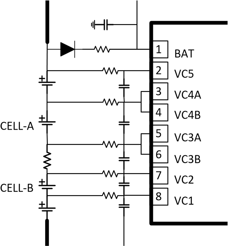
If the BQ76922 device is used in a system with fewer than 5-series cells, the additional cell inputs can be utilized to improve measurement performance. For example, a long connection may exist between two cells in a pack, such that there may be significant interconnect resistance between the cells, such as shown in Figure 4-1 between CELL-A and CELL-B. By connecting VC2 close to the positive terminal of CELL-B, and connecting VC3B close to the negative terminal of CELL-A, more accurate cell voltage measurements are obtained for CELL-A and CELL-B, since the I·R voltage across the interconnect resistance between the cells is not included in either cell voltage measurement. Since the device reports the voltage across the interconnect resistance and the synchronized current in DASTATUS1–2(), the resistance of the interconnect between CELL-A and CELL-B can also be calculated and monitored during operation. It is recommended to include the series resistance and bypass capacitor on cell inputs connected in this manner, as shown below.
 Figure 4-1 Using
Cell
Input
Pins
for
Interconnect
Measurement
Figure 4-1 Using
Cell
Input
Pins
for
Interconnect
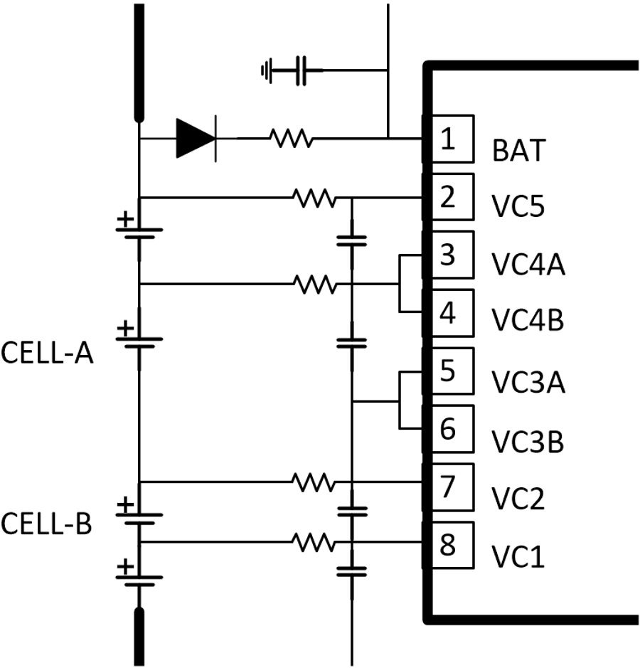
MeasurementIf this connection across an interconnect is not needed (or it is preferred to avoid the extra resistor and capacitor), then the unused cell input pins should be shorted to adjacent cell input pins, as shown in Figure 4-2 for VC3B.
 Figure 4-2 Terminating an
Unused
Cell
Input
Pin
Figure 4-2 Terminating an
Unused
Cell
Input
PinThe Settings:Configuration:Vcell Mode configuration register is used to specify which cell inputs are used for actual cells. The device uses this information to disable cell voltage protections associated with inputs that are used to measure interconnect or are not used at all. Voltage measurements for all inputs are reported in a 16-bit format (in units of mV) as well as a 32-bit format (in units of raw ADC counts), irrespective of whether they are used for cells or not.