SLVA927A November 2017 – April 2019 LM25066A , LM25066I , LM5050-1 , LM5051 , LM5064 , LM5066 , LM5067 , LM5069 , LM66100 , LM74500-Q1 , LM74700-Q1 , TPL7407LA , TPS1H100-Q1 , TPS1HA08-Q1 , TPS2113A , TPS2115A , TPS22810 , TPS22915 , TPS22916 , TPS22918 , TPS22971 , TPS22990 , TPS23525 , TPS2412 , TPS24751 , TPS24770 , TPS25942A , TPS2595 , TPS2660 , TPS27S100 , TPS2H160-Q1 , TPS4H160-Q1 , ULN2003A
1 Load Switches
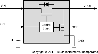
 Figure 2. Load Switch Block Diagram
 Integrated load switches are electronic switches that turn power rails on and off. When the internal FET turns on, current flows from the input to output and passes power to the downstream circuitry. When the device is enabled, the rise time of the output voltage (VOUT) can be controlled by adjusting the capacitance on an external pin (CT pin). When the device is disabled, the fall time of VOUT is controlled through the quick output discharge (QOD). QOD pulls the output to ground whenever the device is turned off, preventing the output from floating or entering an undetermined state.
Some common functions of load switches include power savings, power sequencing, and inrush current control. Power savings is important in applications looking to minimize current dissipation and maximize power efficiency. By disconnecting the supply from a load or subsystem, the switch minimizes power drawn from inactive loads. Power sequencing is important in applications where individual voltage rails need to be turned on and off in a specific order. By configuring the CT and QOD pins, the ramp-up and power-down timing can be adjusted. Inrush current control protects systems that contain large bulk capacitors near the load. When power is initially applied to the system, charging these capacitors can result in a large inrush current that exceeds the nominal load current. If left unaddressed, this can cause voltage rails to fall out of regulation due to the drop, resulting in the system entering an undesired state. Load switches can mitigate the inrush current by using the CT pin to manage the rise time of the power rail. This leads to a linear output slew rate with no voltage dips or external regulators required.
Table 2. Load Switch Examples(1)
| DESCRIPTION | DEVICES | VOLTAGE RANGE | MAX CURRENT | TYPICAL Ron | PACKAGE |
|---|---|---|---|---|---|
| Adjustable rise time, adjustable QOD | TPS22918 | 1 V to 5.5 V | 2 A | 52 mΩ | SOT |
| TPS22810 | 2.7 V to 18 V | 2 A | 79 mΩ | SOT | |
| Space-constrained applications | TPS22915 | 1.05 V to 5.5 V | 2 A | 37 mΩ | CSP |
| TPS22916 | 1 V to 5.5 V | 2 A | 60 mΩ | CSP | |
| Self protected with controlled rise time | TPS22919 | 1.6 V to 5.5 V | 1.5 A | 90 mΩ | SOT |
| Lowest ON-resistance, power good indication | TPS22990 | 1 V to 5.5 V | 10 A | 3.9 mΩ | SON |
| Fast turn-on time (≤ 65 µs), Power Good indication, QOD, thermal shutdown | TPS22971 | 0.65 V to 3.6 V | 3 A | 6.7 mΩ | DSBGA |