SLVAE69 July 2019 TPS568215 , TPS56C215
3.2 Bench Waveforms
Figure 6 through Figure 13 show TPS56C215 steady state, start up, shut down and ORing switch waveforms. It indicates that with external VREG5 power supply, TPS56C215 could support applications with input voltages as low as 4 V. 5 V and 12 V rails switches can be realized smoothly
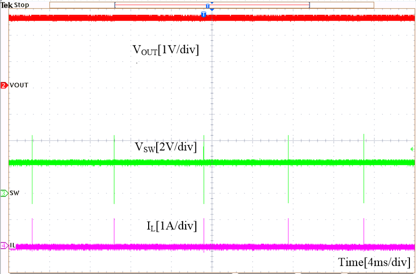 Figure 6. Steady State, VIN= 4 V, IOUT= 0 A
  Figure 7. Steady State, VIN= 4 V, IOUT= 12 A
 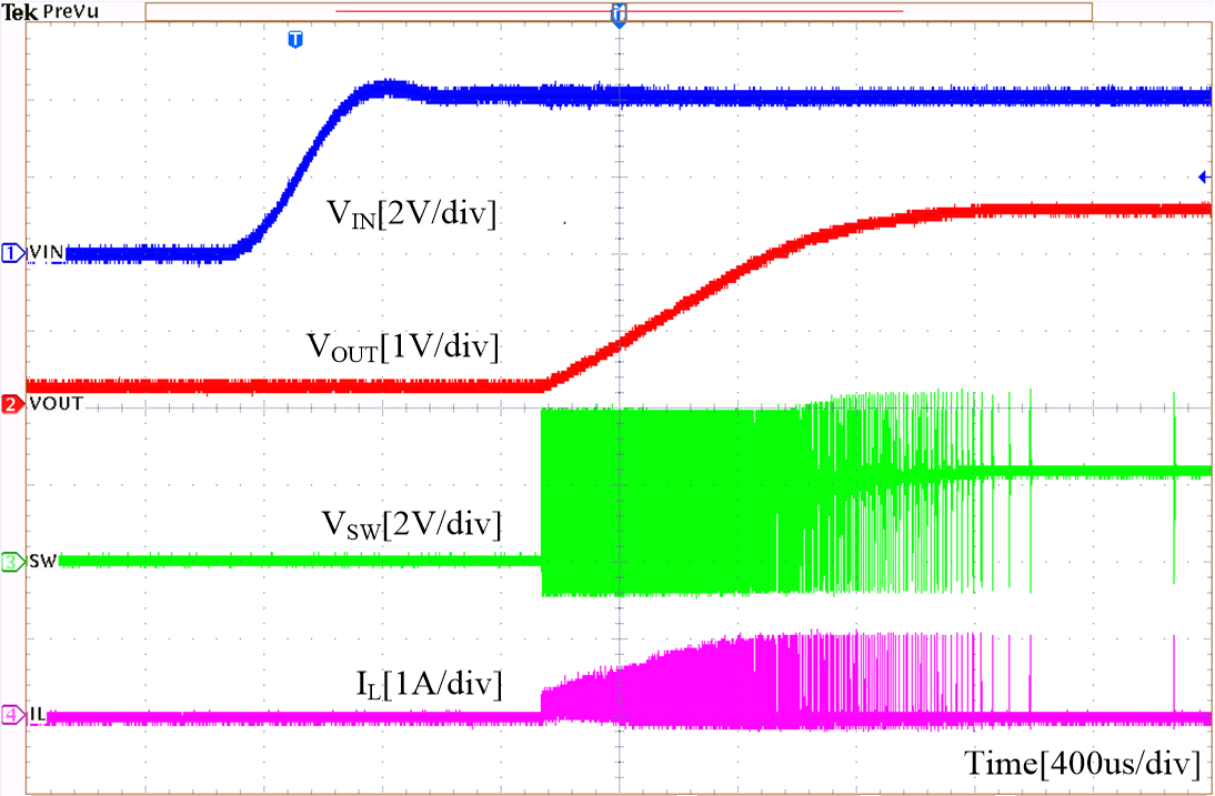 Figure 8. Start Up, VIN= 4 V, IOUT= 0 A
 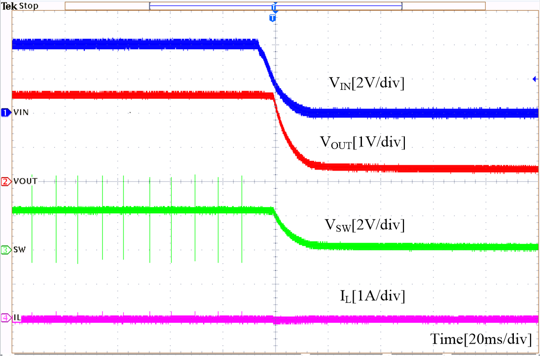 Figure 9. Shut Down, VIN= 4 V, IOUT= 0 A
 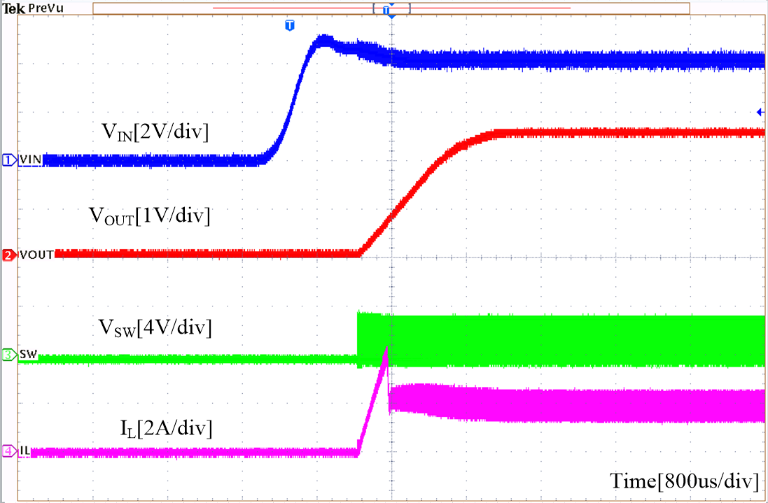 Figure 10. Start Up, VIN= 4 V, IOUT= 2 A
  Figure 11. Shut Down, VIN= 4 V, IOUT= 2 A
 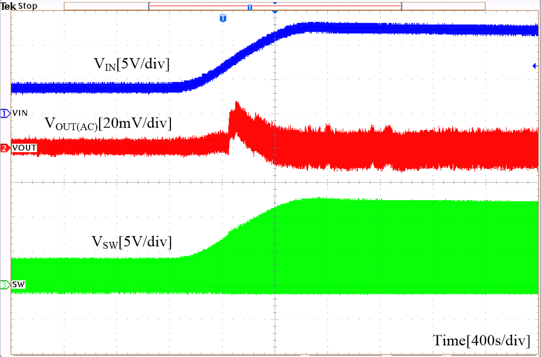 Figure 12. O-ring Switch, VIN 5 V to 12 V, IOUT= 2 A
  Figure 13. O-ring Switch, VIN 12 V to 5 V, IOUT= 2 A