SLVAE69 July 2019 TPS568215 , TPS56C215
3 Schematic and Bench Results
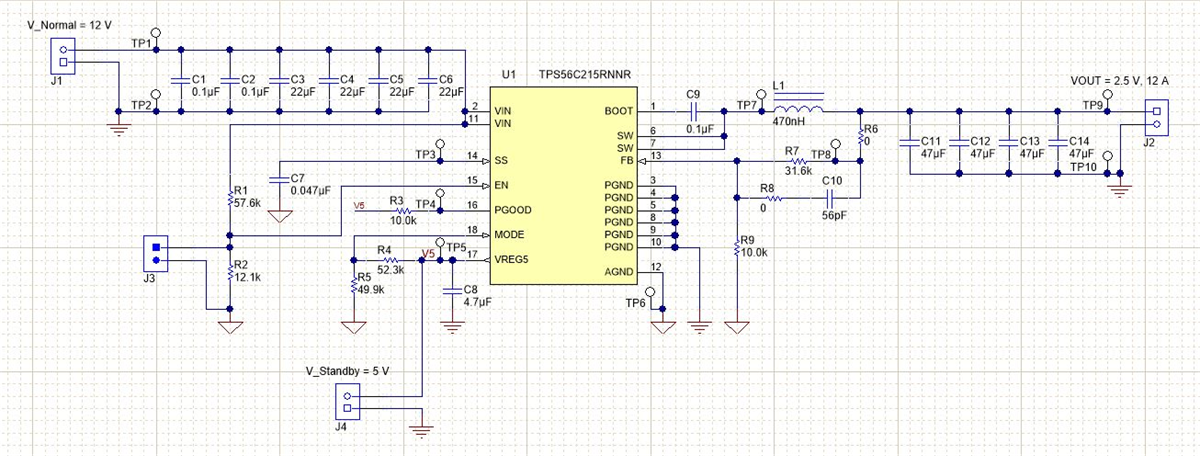
The detail schematic of external VREG5 Biased TPS56C215 schematic is shown in Figure 4.
 Figure 4. External VREG5 Biased TPS56C215 Schematic
 The system level parameters are shown in Table 1.
Table 1. System Parameters
| Parameter | Example Value |
|---|---|
| 12 V Input Voltage Rail, V 12 | 12 VDC |
| 5 V Input Voltage Rail, V 5 | 5 VDC |
| VREG5 Supply, VDD | 5 VDC |
| Output VPP Voltage, VOUT | 2.5 VDC |
| Maximum Output Current, IO_MAX | 12 A |
| Switching Frequency, FSW | 800 kHz |
| Output Inductor, Lf | 470 nH |
| Output Capacitor, COUT | 47uFx4 |