SLVAEK8B December 2019 – November 2024 LP2951-Q1
4.1 WSON-8 Package
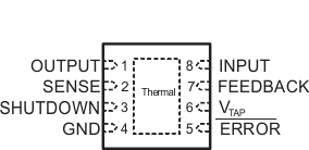
Figure 4-1 shows the LP2951-Q1 pin diagram for the WSON-8 package. For a detailed description of the device pins, see the Pin Configuration and Functions section in the LP2951-Q1 data sheet.
 Figure 4-1 Pin Diagram (WSON-8) Package
Table 4-2 Pin FMA for Device Pins
Short-Circuited to Ground
| Pin Name | Pin No. | Description of Potential Failure Effects | Failure Effect Class |
|---|---|---|---|
| Output | 1 | Regulation is not possible, the device operates at current limit. The device can cycle in an out of thermal shutdown. | B |
| Sense | 2 | Regulation is not possible, the device operates at current limit. | B |
| Shutdown | 3 | Proper regulation without the ability to shutdown device. | B |
| GND | 4 | No effect. Normal operation. | D |
| Error | 5 | Proper regulation without the ability to error output. | B |
| VTAP | 6 | (Fixed) Output is pulled low, leading to undesired fixed output. | B |
| (Adjustable) No effect. Normal operation. | D | ||
| Feedback | 7 | (Fixed) Output is pulled low, leading to undesired fixed output. | B |
| (Adjustable) Output is pulled low, leading to an undesired output. | B | ||
| Input | 8 | Power is not supplied to the device. System performance depends on upstream current limiting. | B |
Table 4-3 Pin FMA for Device Pins
Open-Circuited
| Pin Name | Pin No. | Description of Potential Failure Effects | Failure Effect Class |
|---|---|---|---|
| Output | 1 | The device output is disconnected from the load. | B |
| Sense | 2 | Unable to sense the output, leading to an unknown output state | B |
| Shutdown | 3 | The device is in the low-power shutdown state if left floating. | B |
| GND | 4 | There is no current loop for the supply voltage. The device is not operational and does not regulate. | B |
| Error | 5 | No effect. Normal operation. | D |
| VTAP | 6 | (Fixed) There is no connection to feedback, leading to an undesired output. | B |
| (Adjustable) No effect. Normal operation. | D | ||
| Feedback | 7 | There is no connection to feedback, leading to an undesired output. | B |
| (Adjustable) Input to device error amplifier is left floating, leading to an undesired output. | B | ||
| Input | 8 | Power is not supplied to the device. | B |
Table 4-4 Pin FMA for Device Pins
Short-Circuited to Adjacent Pin
| Pin Name | Pin No. | Shorted to | Description of Potential Failure Effects | Failure Effect Class |
|---|---|---|---|---|
| Output | 1 | Sense | No effect. Normal operation. | D |
| Sense | 2 | Shutdown | Output pin is driven low. | B |
| Shutdown | 3 | GND | Proper regulation without the ability to shutdown device. | B |
| Error | 5 | VTAP | The device state is unknown, leading to an inaccurate reading of the output. | B |
| VTAP | 6 | Feedback | (Fixed) No effect. Normal operation. | D |
| (Adjustable) Unable to use external feedback resistors, leading to an undesired output. | B | |||
| Feedback | 7 | Input | Device can become damaged as feedback is low voltage and input is high voltage. | A |
Table 4-5 Pin FMA for Device Pins
Short-Circuited to
Input
| Pin Name | Pin No. | Description of Potential Failure Effects | Failure Effect Class |
|---|---|---|---|
| Output | 1 | Regulation is not possible, leading to an undesired output state. | B |
| Sense | 2 | Device can become damaged. | A |
| Shutdown | 3 | The device is in the shutdown state. | B |
| GND | 4 | Power is not supplied to the device. System performance depends on upstream current limiting. | B |
| Error | 5 | The device state is unknown leading to an inaccurate reading of the output. | B |
| VTAP | 6 | Device can become damaged. | A |
| Feedback | 7 | Device can become damaged. | A |
| Input | 8 | No effect. Normal operation. | D |